- 您现在的位置:买卖IC网 > PDF目录2067 > CY28329ZXC (Silicon Laboratories Inc)IC CLOCK CK408B PLUMAS 56SSOP PDF资料下载
参数资料
| 型号: | CY28329ZXC |
| 厂商: | Silicon Laboratories Inc |
| 文件页数: | 11/16页 |
| 文件大小: | 0K |
| 描述: | IC CLOCK CK408B PLUMAS 56SSOP |
| 标准包装: | 35 |
| 类型: | * |
| PLL: | 是 |
| 输入: | 晶体 |
| 输出: | 时钟 |
| 电路数: | 1 |
| 比率 - 输入:输出: | 1:24 |
| 差分 - 输入:输出: | 无/是 |
| 频率 - 最大: | 133MHz |
| 除法器/乘法器: | 无/无 |
| 电源电压: | 3.135 V ~ 3.465 V |
| 工作温度: | 0°C ~ 70°C |
| 安装类型: | * |
| 封装/外壳: | * |
| 供应商设备封装: | * |
| 包装: | * |
| 其它名称: | SLCY28329ZXC |
CY28329
....................... Document #: 38-07040 Rev. *E Page 4 of 16
Serial Data Interface (SMBus)
To enhance the flexibility and function of the clock synthesizer,
a two-signal SMBus interface is provided according to SMBus
specification. Through the Serial Data Interface, various
device functions such as individual clock output buffers, etc.
can be individually enabled or disabled. CY28329 support
both block read and block write operations.
The registers associated with the Serial Data Interface
initializes to its default setting upon power-up, and therefore
use of this interface is optional. Clock device register changes
are normally made upon system initialization, if any are
required. The interface can also be used during system
operation for power management functions.
Data Protocol
The clock driver serial protocol accepts only Block Writes from
the controller. The bytes must be accessed in sequential order
from lowest to highest byte, (most significant bit first) with the
ability to stop after any complete byte has been transferred.
Indexed bytes are not allowed.
A Block write begins with a slave address and a WRITE
condition. The R/W bit is used by the SMBus controller as a
data direction bit. A zero indicates a WRITE condition to the
clock device. The slave receiver address is 11010010 (D2h).
A command code of 0000 0000 (00h) and the byte count bytes
are required for any transfer. After the command code, the
core logic issues a byte count, which describes number of
additional bytes required for the transfer, not including the
command code and byte count bytes. For example, if the host
has 20 data bytes to send, the first byte would be the number
20 (14h), followed by the 20 bytes of data. The byte count byte
is required to be a minimum of 1 byte and a maximum of 32
bytes It may not be 0. Figure 1 shows an example of a block
write.
A transfer is considered valid after the acknowledge bit corre-
sponding to the byte count is read by the controller.
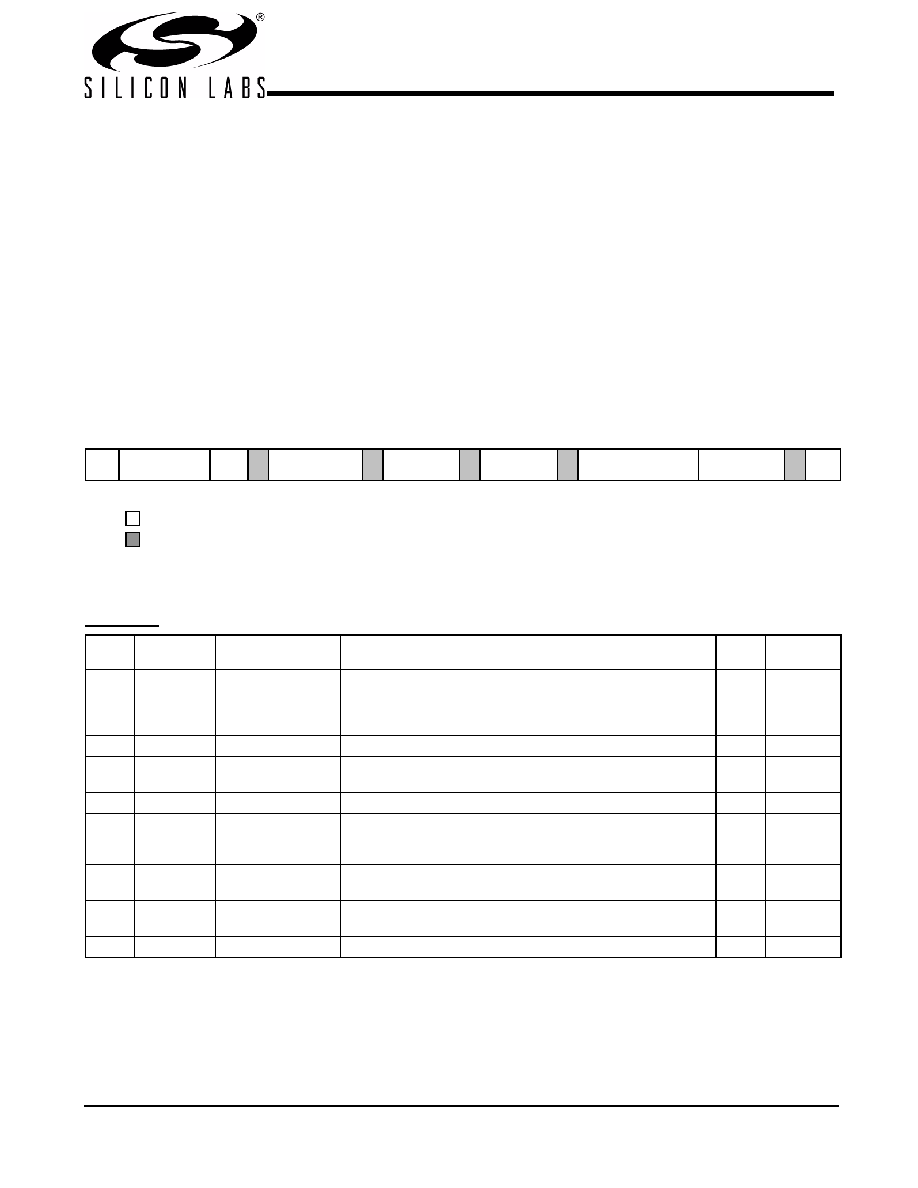
Data Byte Configuration Map
Start
bit
Slave Address
1 1 0 1 0 0 1 0
R/W
0/1
A Command Code
0 0 0 0 0 0 0 0
A Byte Count =
N
A
Data Byte 0
A
. . .
Data Byte N-1
A
Stop
bit
1 bit
7 bits
1
8 bits
1
8 bits
1
8 bits
1
8 bits
1
1 bit
Figure 1. An Example of a Block Write
From Master to Slave
From Slave to Master
Data Byte 0: Control Register (0 = Enable, 1 = Disable)
Bit
Affected
Pin#
Name
Description
Type
Power On
Default
Bit 7
5, 6, 7, 10,
11, 12, 13,
16, 17, 18,
33, 35
PCI [0:6]
CPU[3:0]
3V66[1:0]
Spread Spectrum Enable
0 = Spread Off, 1 = Spread On
R/W
0
Bit 6
–
Reserved, set = 0
R
0
Bit 5
35
3V66_1/VCH
VCH Select 66 MHz/48 MHz
0 = 66 MHz, 1 = 48 MHz
R/W
0
Bit 4
–
Reserved
R
1
Bit 3
10, 11, 12,
13, 16, 17,
18
PCI [6:0]
PCI_STOP#, 0 = stopped, 1 = running
(Does not affect PCI_F [2:0] pins)
R/W
1
Bit 2
40
S2
Reflects the value of the S2 pin sampled on Power-up
RHW
Bit 1
55
S1
Reflects the value of the S1 pin sampled on Power-up
RHW
Bit 0
–
Reserved
R
1
相关PDF资料 |
PDF描述 |
|---|---|
| CY28346OXC | IC CLOCK DIFF OUT CK408 56SSOP |
| CY28346ZI-2 | IC CLOCK DIFF OUT CK408 56TSSOP |
| CY28353OXC-2 | IC CLOCK DIFF/DRIVER PLL 28TSSOP |
| CY28409OXC | IC CLOCK CK409GRANTSDALE 56TSSOP |
| CY28419ZXC | IC CLOCK SERV CK419 56TSSOP |
相关代理商/技术参数 |
参数描述 |
|---|---|
| CY28329ZXCT | 功能描述:时钟驱动器及分配 Intel CK-408B for Plumas chipset RoHS:否 制造商:Micrel 乘法/除法因子:1:4 输出类型:Differential 最大输出频率:4.2 GHz 电源电压-最大: 电源电压-最小:5 V 最大工作温度:+ 85 C 封装 / 箱体:SOIC-8 封装:Reel |
| CY2833 | 制造商:CYPRESS 制造商全称:Cypress Semiconductor 功能描述:Intel CK408 Mobile Clock Synthesizer |
| CY28330 | 制造商:CYPRESS 制造商全称:Cypress Semiconductor 功能描述:Clock Generator for AMD⑩ Hammer |
| CY28330OC | 制造商:Cypress Semiconductor 功能描述: |
| CY28330OCT | 制造商:CYPRESS 制造商全称:Cypress Semiconductor 功能描述:Clock Generator for AMD⑩ Hammer |
发布紧急采购,3分钟左右您将得到回复。