- 您现在的位置:买卖IC网 > PDF目录9026 > CY28346ZXC-2 (Silicon Laboratories Inc)IC CLOCK DIFF OUT CK408 56TSSOP PDF资料下载
参数资料
| 型号: | CY28346ZXC-2 |
| 厂商: | Silicon Laboratories Inc |
| 文件页数: | 13/19页 |
| 文件大小: | 0K |
| 描述: | IC CLOCK DIFF OUT CK408 56TSSOP |
| 标准包装: | 35 |
| 类型: | * |
| PLL: | 是 |
| 输入: | 晶体 |
| 输出: | 时钟 |
| 电路数: | 1 |
| 比率 - 输入:输出: | 1:21 |
| 差分 - 输入:输出: | 无/是 |
| 频率 - 最大: | 200MHz |
| 除法器/乘法器: | 是/无 |
| 电源电压: | 3.135 V ~ 3.465 V |
| 工作温度: | 0°C ~ 70°C |
| 安装类型: | * |
| 封装/外壳: | * |
| 供应商设备封装: | * |
| 包装: | * |
CY28346-2
........................ Document #: 38-07509 Rev. *B Page 3 of 19
Serial Data Interface
To enhance the flexibility and function of the clock synthesizer,
a two-signal serial interface is provided. Through the Serial
Data Interface, various device functions, such as individual
clock output buffers, can be individually enabled or disabled.
The registers associated with the Serial Data Interface
initializes to their default setting upon power-up, and therefore
use of this interface is optional. Clock device register changes
are normally made upon system initialization, if any are
required. The interface can also be used during system
operation for power management functions.
Data Protocol
The clock driver serial protocol accepts block write and block
read operations from the controller. For block write/read
operation, the bytes must be accessed in sequential order
from lowest to highest byte (most significant bit first) with the
ability to stop after any complete byte has been transferred.
The block write and block read protocol is outlined in Table 2.
The slave receiver address is 11010010 (D2h).
41
VSSIREF
–
PWR Current reference programming input for CPU buffers. A resistor is
connected between this pin and IREF. This pin should also be returned
to device VSS.
26
VDDA
–
PWR Analog power input. Used for PLL and internal analog circuits. It is also
specifically used to detect and determine when power is at an acceptable
level to enable the device to operate.
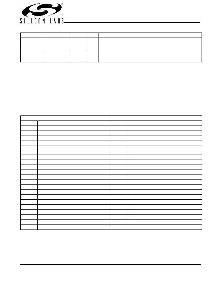
Pin Description (continued)
Pin
Name
PWR
I/O
Description
Table 2. Block Read and Block Write Protocol
Block Write Protocol
Block Read Protocol
Bit
Description
Bit
Description
1Start
1
Start
2:8
Slave address – 7 bits
2:8
Slave address – 7 bits
9
Write = 0
9
Write = 0
10
Acknowledge from slave
10
Acknowledge from slave
11:18
Command Code – 8 bit
‘00000000’ stands for block operation
11:18
Command Code – 8 bit
‘00000000’ stands for block operation
19
Acknowledge from slave
19
Acknowledge from slave
20:27
Byte Count – 8 bits
20
Repeat start
28
Acknowledge from slave
21:27
Slave address – 7 bits
29:36
Data byte 1 – 8 bits
28
Read = 1
37
Acknowledge from slave
29
Acknowledge from slave
38:45
Data byte 2 – 8 bits
30:37
Byte count from slave – 8 bits
46
Acknowledge from slave
38
Acknowledge
....
......................
39:46
Data byte from slave – 8 bits
....
Data Byte (N–1) –8 bits
47
Acknowledge
....
Acknowledge from slave
48:55
Data byte from slave – 8 bits
....
Data Byte N –8 bits
56
Acknowledge
....
Acknowledge from slave
....
Data bytes from slave/Acknowledge
....
Stop
....
Data byte N from slave – 8 bits
....
Not Acknowledge
....
Stop
相关PDF资料 |
PDF描述 |
|---|---|
| CY28346ZXC | IC CLOCK DIFF OUT CK408 56TSSOP |
| VE-B32-MV-F2 | CONVERTER MOD DC/DC 15V 150W |
| VE-B32-MV-F1 | CONVERTER MOD DC/DC 15V 150W |
| VE-B31-MV-F4 | CONVERTER MOD DC/DC 12V 150W |
| ICS525RI-11LF | IC PECL CLK USER CONFIG 28-SSOP |
相关代理商/技术参数 |
参数描述 |
|---|---|
| CY28346ZXC-2T | 功能描述:时钟合成器/抖动清除器 NB Clk Intel Brkdale 830M & 845 chipsets RoHS:否 制造商:Skyworks Solutions, Inc. 输出端数量: 输出电平: 最大输出频率: 输入电平: 最大输入频率:6.1 GHz 电源电压-最大:3.3 V 电源电压-最小:2.7 V 封装 / 箱体:TSSOP-28 封装:Reel |
| CY28346ZXCT | 功能描述:时钟合成器/抖动清除器 NB Clk Intel Brkdale 830M & 845 chipsets RoHS:否 制造商:Skyworks Solutions, Inc. 输出端数量: 输出电平: 最大输出频率: 输入电平: 最大输入频率:6.1 GHz 电源电压-最大:3.3 V 电源电压-最小:2.7 V 封装 / 箱体:TSSOP-28 封装:Reel |
| CY28347 | 制造商:CYPRESS 制造商全称:Cypress Semiconductor 功能描述:Universal Single-chip Clock Solution for VIA P4M266/KM266 DDR Systems |
| CY28347OC | 制造商:CYPRESS 制造商全称:Cypress Semiconductor 功能描述:Universal Single-chip Clock Solution for VIA P4M266/KM266 DDR Systems |
| CY28347OCT | 制造商:CYPRESS 制造商全称:Cypress Semiconductor 功能描述:Universal Single-chip Clock Solution for VIA P4M266/KM266 DDR Systems |
发布紧急采购,3分钟左右您将得到回复。