- 您现在的位置:买卖IC网 > PDF目录1992 > CY284108ZXC (Silicon Laboratories Inc)IC CLOCK SERV CK410B 56TSSOP PDF资料下载
参数资料
| 型号: | CY284108ZXC |
| 厂商: | Silicon Laboratories Inc |
| 文件页数: | 10/16页 |
| 文件大小: | 0K |
| 描述: | IC CLOCK SERV CK410B 56TSSOP |
| 标准包装: | 35 |
| 类型: | 时钟/频率发生器 |
| PLL: | 是 |
| 主要目的: | Intel CPU 服务器 |
| 输入: | 晶体 |
| 输出: | HCSL,LVCMOS |
| 电路数: | 1 |
| 比率 - 输入:输出: | 1:19 |
| 差分 - 输入:输出: | 无/是 |
| 频率 - 最大: | 400MHz |
| 电源电压: | 3.135 V ~ 3.465 V |
| 工作温度: | 0°C ~ 70°C |
| 安装类型: | 表面贴装 |
| 封装/外壳: | 56-TFSOP(0.240",6.10mm 宽) |
| 供应商设备封装: | 56-TSSOP |
| 包装: | 管件 |
CY284108
........................ Document #: 38-07713 Rev. *B Page 3 of 16
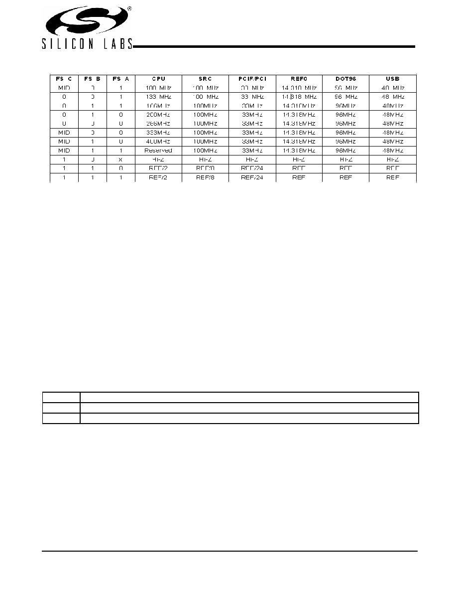
Table 1. CPU Frequency Select Tables
Frequency Select Pins (FS_[C:A])
Host clock frequency selection is achieved by applying the
appropriate logic levels to FS_A, FS_B, FS_C inputs prior to
VTT_PWRGD# assertion (as seen by the clock synthesizer).
Upon VTT_PWRGD# being sampled low by the clock chip
(indicating processor VTT voltage is stable), the clock chip
samples the FS_A, FS_B, and FS_C input values. For all logic
levels of FS_A, FS_B, and FS_C, VTT_PWRGD# employs a
one-shot
functionality
in
that
once
a
valid
low
on
VTT_PWRGD# has been sampled, all further VTT_PWRGD#,
FS_A, FS_B, and FS_C transitions will be ignored, except in
test mode. FS_C is a three level input, when sampled at a
voltage greater than 2.0V by VTTPWRGD#, the device will
enter test mode as selected by the voltage level on the FS_B
input.
Serial Data Interface
To enhance the flexibility and function of the clock synthesizer,
a two-signal serial interface is provided. Through the Serial
Data Interface, various device functions, such as individual
clock output buffers, can be individually enabled or disabled.
The registers associated with the Serial Data Interface
initialize to their default setting upon power-up, and therefore
use of this interface is optional. Clock device register changes
are normally made upon system initialization, if any are
required. The interface cannot be used during system
operation for power management functions.
Data Protocol
The clock driver serial protocol accepts byte write, byte read,
block write, and block read operations from the controller. For
block write/read operation, the bytes must be accessed in
sequential order from lowest to highest byte (most significant
bit first) with the ability to stop after any complete byte has
been transferred. For byte write and byte read operations, the
system controller can access individually indexed bytes. The
offset of the indexed byte is encoded in the command code,
as described in Table 2.
The block write and block read protocol is outlined in Table 3
while Table 4 outlines the corresponding byte write and byte
read protocol. The slave receiver address is 11010010 (D2h).
Table 2. Command Code Definition
Bit
Description
7
0 = Block read or block write operation, 1 = Byte read or byte write operation
(6:0)
Byte offset for byte read or byte write operation. For block read or block write operations, these bits should be '0000000'
相关PDF资料 |
PDF描述 |
|---|---|
| CY28410OXC-2 | IC CLOCK CK410 GRANTSDALE 56SSOP |
| CY28410OXC | IC CLOCK CK410 GRANTSDALE 56SSOP |
| CY28411ZXC | IC CLOCK CK410M ALVISO 56TSSOP |
| CY28442ZXC-2 | IC CLOCK ALVISO PENTM 56TSSOP |
| CY28445LFXC-5 | IC CLOCK CALISTOGA CK410M 68QFN |
相关代理商/技术参数 |
参数描述 |
|---|---|
| CY284108ZXCT | 功能描述:时钟发生器及支持产品 Server, CK410B RoHS:否 制造商:Silicon Labs 类型:Clock Generators 最大输入频率:14.318 MHz 最大输出频率:166 MHz 输出端数量:16 占空比 - 最大:55 % 工作电源电压:3.3 V 工作电源电流:1 mA 最大工作温度:+ 85 C 安装风格:SMD/SMT 封装 / 箱体:QFN-56 |
| CY28410OC | 制造商:SPECTRALINEAR 制造商全称:SPECTRALINEAR 功能描述:Clock Generator for Intel Grantsdale Chipset |
| CY28410OCT | 制造商:SPECTRALINEAR 制造商全称:SPECTRALINEAR 功能描述:Clock Generator for Intel Grantsdale Chipset |
| CY28410OXC | 功能描述:时钟发生器及支持产品 SysClk Intel Lakeprt & Grantsdale Chipset RoHS:否 制造商:Silicon Labs 类型:Clock Generators 最大输入频率:14.318 MHz 最大输出频率:166 MHz 输出端数量:16 占空比 - 最大:55 % 工作电源电压:3.3 V 工作电源电流:1 mA 最大工作温度:+ 85 C 安装风格:SMD/SMT 封装 / 箱体:QFN-56 |
| CY28410OXC-2 | 功能描述:时钟发生器及支持产品 SysClk Intel Lakeprt & Grantsdale Chipset RoHS:否 制造商:Silicon Labs 类型:Clock Generators 最大输入频率:14.318 MHz 最大输出频率:166 MHz 输出端数量:16 占空比 - 最大:55 % 工作电源电压:3.3 V 工作电源电流:1 mA 最大工作温度:+ 85 C 安装风格:SMD/SMT 封装 / 箱体:QFN-56 |
发布紧急采购,3分钟左右您将得到回复。