- 您现在的位置:买卖IC网 > PDF目录1992 > CY28410OXC-2 (Silicon Laboratories Inc)IC CLOCK CK410 GRANTSDALE 56SSOP PDF资料下载
参数资料
| 型号: | CY28410OXC-2 |
| 厂商: | Silicon Laboratories Inc |
| 文件页数: | 15/16页 |
| 文件大小: | 0K |
| 描述: | IC CLOCK CK410 GRANTSDALE 56SSOP |
| 标准包装: | 26 |
| 类型: | 时钟/频率发生器 |
| PLL: | 是 |
| 主要目的: | Intel CPU 服务器 |
| 输入: | 晶体 |
| 输出: | HCSL,LVCMOS |
| 电路数: | 1 |
| 比率 - 输入:输出: | 1:21 |
| 差分 - 输入:输出: | 无/是 |
| 频率 - 最大: | 266MHz |
| 电源电压: | 3.135 V ~ 3.465 V |
| 工作温度: | 0°C ~ 70°C |
| 安装类型: | 表面贴装 |
| 封装/外壳: | 56-BSSOP(0.295",7.50mm 宽) |
| 供应商设备封装: | 56-SSOP |
| 包装: | 管件 |
CY28410-2
........................Document #: 38-07747 Rev *.* Page 8 of 16
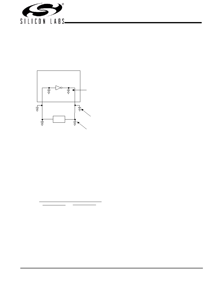
Calculating Load Capacitors
In addition to the standard external trim capacitors, trace
capacitance and pin capacitance must also be considered to
correctly calculate crystal loading. As mentioned previously,
the capacitance on each side of the crystal is in series with the
crystal. This means the total capacitance on each side of the
crystal must be twice the specified crystal load capacitance
(CL). While the capacitance on each side of the crystal is in
series with the crystal, trim capacitors (Ce1,Ce2) should be
calculated to provide equal capacitive loading on both sides.
As mentioned previously, the capacitance on each side of the
crystal is in series with the crystal. This means the total capac-
itance on each side of the crystal must be twice the specified
load capacitance (CL). While the capacitance on each side of
the crystal is in series with the crystal, trim capacitors
(Ce1,Ce2) should be calculated to provide equal capacitance
loading on both sides.
Use the following formulas to calculate the trim capacitor
values for Ce1 and Ce2.
CL ................................................... Crystal load capacitance
CLe .........................................Actual loading seen by crystal
using standard value trim capacitors
Ce .....................................................External trim capacitors
Cs ............................................. Stray capacitance (terraced)
Ci .......................................................... Internal capacitance
(lead frame, bond wires etc.)
PD (Power-down) Clarification
The VTT_PWRGD# /PD pin is a dual-function pin. During
initial power-up, the pin functions as VTT_PWRGD#. Once
VTT_PWRGD# has been sampled LOW by the clock chip, the
pin assumes PD functionality. The PD pin is an asynchronous
active HIGH input used to shut off all clocks cleanly prior to
shutting off power to the device. This signal is synchronized
internal to the device prior to powering down the clock synthe-
sizer. PD is also an asynchronous input for powering up the
system. When PD is asserted HIGH, all clocks are driven to a
low value and held prior to turning off the VCOs and the crystal
oscillator.
PD (Power-down) – Assertion
When PD is sampled HIGH by two consecutive rising edges
of CPUC, all single-ended outputs will be held LOW on their
next HIGH-to-LOW transition and differential clocks must be
held HIGH or Hi-Z (depending on the state of the control
register drive mode bit) on the next diff clock# HIGH-to-LOW
transition within 4 clock periods. When the SMBus PD drive
mode bit corresponding to the differential (CPU, SRC, and
DOT) clock output of interest is programmed to ‘0’, the clock
output must be held with “Diff clock” pin driven HIGH at 2 x Iref,
and “Diff clock#” tri-state. If the control register PD drive mode
bit corresponding to the output of interest is programmed to
“1”, then both the “Diff clock” and the “Diff clock#” are Hi-Z.
Note the example below shows CPUT = 133 MHz and PD
drive mode = ‘1’ for all differential outputs. Figure 3 and this
description is applicable to valid CPU frequencies 100, 133,
166, 200, 266, 333, and 400 MHz. In the event that PD mode
is desired as the initial power-on state, PD must be asserted
high in less than 10
s after asserting VTT_PWRGD#.
PD Deassertion
The power-up latency is less than 1.8 ms. This is the time from
the deassertion of the PD pin or the ramping of the power
supply until the time that stable clocks are output from the
clock chip. All differential outputs stopped in a three-state
condition resulting from power-down must be driven HIGH in
less than 300
s of PD deassertion to a voltage greater than
200 mV. After the clock chip’s internal PLL is powered up and
locked, all outputs are enabled within a few clock cycles of
XTAL
Ce2
Ce1
Cs1
Cs2
X1
X2
Ci1
Ci2
Clock Chip
Trace
2.8pF
Trim
33pF
Pin
3 to 6p
Figure 2. Crystal Loading Example
Load Capacitance (each side)
Total Capacitance (as seen by the crystal)
Ce = 2 * CL – (Cs + Ci)
Ce1 + Cs1 + Ci1
1
+
Ce2 + Cs2 + Ci2
1
()
1
=
CLe
相关PDF资料 |
PDF描述 |
|---|---|
| CY28410OXC | IC CLOCK CK410 GRANTSDALE 56SSOP |
| CY28411ZXC | IC CLOCK CK410M ALVISO 56TSSOP |
| CY28442ZXC-2 | IC CLOCK ALVISO PENTM 56TSSOP |
| CY28445LFXC-5 | IC CLOCK CALISTOGA CK410M 68QFN |
| CY28446LFXC | IC CLOCK CALISTOGA CK410M 64QFN |
相关代理商/技术参数 |
参数描述 |
|---|---|
| CY28410OXC-2T | 功能描述:时钟发生器及支持产品 SysClk Intel Lakeprt & Grantsdale Chipset RoHS:否 制造商:Silicon Labs 类型:Clock Generators 最大输入频率:14.318 MHz 最大输出频率:166 MHz 输出端数量:16 占空比 - 最大:55 % 工作电源电压:3.3 V 工作电源电流:1 mA 最大工作温度:+ 85 C 安装风格:SMD/SMT 封装 / 箱体:QFN-56 |
| CY28410OXCT | 功能描述:时钟发生器及支持产品 SysClk Intel Lakeprt & Grantsdale Chipset RoHS:否 制造商:Silicon Labs 类型:Clock Generators 最大输入频率:14.318 MHz 最大输出频率:166 MHz 输出端数量:16 占空比 - 最大:55 % 工作电源电压:3.3 V 工作电源电流:1 mA 最大工作温度:+ 85 C 安装风格:SMD/SMT 封装 / 箱体:QFN-56 |
| CY28410ZC | 制造商:SPECTRALINEAR 制造商全称:SPECTRALINEAR 功能描述:Clock Generator for Intel Grantsdale Chipset |
| CY28410ZCT | 制造商:SPECTRALINEAR 制造商全称:SPECTRALINEAR 功能描述:Clock Generator for Intel Grantsdale Chipset |
| CY28410ZXC | 功能描述:时钟发生器及支持产品 SysClk Intel Lakeprt & Grantsdale Chipset RoHS:否 制造商:Silicon Labs 类型:Clock Generators 最大输入频率:14.318 MHz 最大输出频率:166 MHz 输出端数量:16 占空比 - 最大:55 % 工作电源电压:3.3 V 工作电源电流:1 mA 最大工作温度:+ 85 C 安装风格:SMD/SMT 封装 / 箱体:QFN-56 |
发布紧急采购,3分钟左右您将得到回复。