- 您现在的位置:买卖IC网 > PDF目录1992 > CY28551LFXC (Silicon Laboratories Inc)IC CLOCK INTEL/AMD SIS VIA 64QFN PDF资料下载
参数资料
| 型号: | CY28551LFXC |
| 厂商: | Silicon Laboratories Inc |
| 文件页数: | 8/28页 |
| 文件大小: | 0K |
| 描述: | IC CLOCK INTEL/AMD SIS VIA 64QFN |
| 标准包装: | 260 |
| 类型: | 时钟/频率发生器 |
| PLL: | 是 |
| 主要目的: | Intel CPU,AMD CPU |
| 输入: | 晶体 |
| 输出: | HCSL,LVCMOS |
| 电路数: | 1 |
| 比率 - 输入:输出: | 1:23 |
| 差分 - 输入:输出: | 无/是 |
| 频率 - 最大: | 400MHz |
| 电源电压: | 3.135 V ~ 3.465 V |
| 工作温度: | 0°C ~ 85°C |
| 安装类型: | 表面贴装 |
| 封装/外壳: | 64-VFQFN 裸露焊盘 |
| 供应商设备封装: | 64-QFN(9x9) |
| 包装: | 托盘 |
第1页第2页第3页第4页第5页第6页第7页当前第8页第9页第10页第11页第12页第13页第14页第15页第16页第17页第18页第19页第20页第21页第22页第23页第24页第25页第26页第27页第28页
CY28551
....................Document #: 001-05675 Rev. *C Page 16 of 28
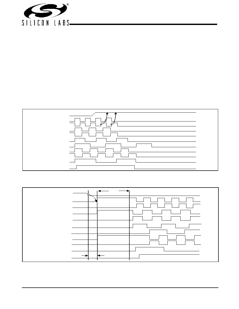
driven to a LOW value and held prior to turning off the VCOs
and the crystal oscillator
PD Assertion
When PD is sampled HIGH by two consecutive rising edges
of CPUC, all single-ended outputs must be held LOW on their
next HIGH-to-LOW transition and differential clocks must be
held HIGH or tri-stated (depending on the state of the control
register drive mode bit) on the next “Diff clock#” HIGH-to-LOW
transition within 4 clock periods. When the SMBus PD drive
mode bit corresponding to the differential (CPU, SRC, and
DOT) clock output of interest is programmed to '0', the clock
output must be held with “Diff clock” pin driven HIGH at 2 x Iref,
and “Diff clock#” tri-state. If the control register PD drive mode
bit corresponding to the output of interest is programmed to ‘1’,
then both the “Diff clock” and the “Diff clock#” are tri-state. Note
Figure 3 shows CPUT = 133 MHz and PD drive mode = '1' for
all differential outputs. This diagram and description is appli-
cable to valid CPU frequencies 100, 133, 166, and 200 MHz.
In the event that PD mode is desired as the initial power-on
state, PD must be asserted HIGH in less than 10
s after
asserting VTT_PWRGD#.
PD Deassertion
The power-up latency must be less than 1.8 ms. This is the
time from the deassertion of the PD pin or the ramping of the
power supply until the time that stable clocks are output from
the clock chip. All differential outputs stopped in a tri-state
condition resulting from power down must be driven HIGH in
less than 300
s of PD deassertion to a voltage greater than
200 mV. After the clock chip's internal PLL is powered up and
locked, all outputs are to be enabled within a few clock cycles
of each other. Figure 4 is an example showing the relationship
of clocks coming up. Unfortunately, we can not show all
possible combinations; designers need to ensure that from the
first active clock output to the last takes no more than two full
PCI clock cycles.
D O T 96C
PD
C P U C , 133 M H z
C P U T , 133 M H z
S R C C 100 M H z
U SB, 4 8 M H z
DO T 9 6 T
S R C T 100 M H z
PC I , 3 3 M H z
RE F
LI N K
Figure 3. PD Assertion Timing Waveform
D O T 96C
PD
CP UC , 1 3 3 M Hz
CP UT , 1 3 3 M Hz
S R CC 1 0 0 M Hz
US B , 4 8 M H z
D O T 96T
SR C T 1 0 0 M H z
Ts t a b le
<1. 8 m s
P C I, 3 3 M H z
RE F
T d r iv e _ P W RDN #
<3 0 0
s > 2 0 0 m V
LI N K
Figure 4. PD Deassertion Timing Waveform
相关PDF资料 |
PDF描述 |
|---|---|
| CY2SSTV855ZXI | IC CLOCK DIFFDRV PLL DDR 28TSSOP |
| CY2SSTV857ZXI-27 | IC CLK DDR266/333BUF1:10 48TSSOP |
| CY2SSTV857ZXI-32 | IC CLK DDR266/333BUF1:10 48TSSOP |
| CY505YC64DT | IC CLK CK505 BROADWATER 64TSSOP |
| CYW150OXC | IC CLOCK 440BX AGP 56SSOP |
相关代理商/技术参数 |
参数描述 |
|---|---|
| CY28551LFXC-3 | 功能描述:时钟发生器及支持产品 Universal System Clk Intel AMD SiS Via RoHS:否 制造商:Silicon Labs 类型:Clock Generators 最大输入频率:14.318 MHz 最大输出频率:166 MHz 输出端数量:16 占空比 - 最大:55 % 工作电源电压:3.3 V 工作电源电流:1 mA 最大工作温度:+ 85 C 安装风格:SMD/SMT 封装 / 箱体:QFN-56 |
| CY28551LFXC-3T | 功能描述:时钟发生器及支持产品 Universal System Clk Intel AMD SiS Via RoHS:否 制造商:Silicon Labs 类型:Clock Generators 最大输入频率:14.318 MHz 最大输出频率:166 MHz 输出端数量:16 占空比 - 最大:55 % 工作电源电压:3.3 V 工作电源电流:1 mA 最大工作温度:+ 85 C 安装风格:SMD/SMT 封装 / 箱体:QFN-56 |
| CY28551LFXCT | 功能描述:时钟发生器及支持产品 Universal System Clk Intel AMD SiS Via RoHS:否 制造商:Silicon Labs 类型:Clock Generators 最大输入频率:14.318 MHz 最大输出频率:166 MHz 输出端数量:16 占空比 - 最大:55 % 工作电源电压:3.3 V 工作电源电流:1 mA 最大工作温度:+ 85 C 安装风格:SMD/SMT 封装 / 箱体:QFN-56 |
| CY2862-000 | 制造商:TE Connectivity 功能描述:82A0111-4-9-G110 |
| CY2863-000 | 制造商:TE Connectivity 功能描述:82A0111-8-9-G110 - Bulk |
发布紧急采购,3分钟左右您将得到回复。