- 您现在的位置:买卖IC网 > PDF目录1992 > CY28551LFXC (Silicon Laboratories Inc)IC CLOCK INTEL/AMD SIS VIA 64QFN PDF资料下载
参数资料
| 型号: | CY28551LFXC |
| 厂商: | Silicon Laboratories Inc |
| 文件页数: | 9/28页 |
| 文件大小: | 0K |
| 描述: | IC CLOCK INTEL/AMD SIS VIA 64QFN |
| 标准包装: | 260 |
| 类型: | 时钟/频率发生器 |
| PLL: | 是 |
| 主要目的: | Intel CPU,AMD CPU |
| 输入: | 晶体 |
| 输出: | HCSL,LVCMOS |
| 电路数: | 1 |
| 比率 - 输入:输出: | 1:23 |
| 差分 - 输入:输出: | 无/是 |
| 频率 - 最大: | 400MHz |
| 电源电压: | 3.135 V ~ 3.465 V |
| 工作温度: | 0°C ~ 85°C |
| 安装类型: | 表面贴装 |
| 封装/外壳: | 64-VFQFN 裸露焊盘 |
| 供应商设备封装: | 64-QFN(9x9) |
| 包装: | 托盘 |
第1页第2页第3页第4页第5页第6页第7页第8页当前第9页第10页第11页第12页第13页第14页第15页第16页第17页第18页第19页第20页第21页第22页第23页第24页第25页第26页第27页第28页
CY28551
....................Document #: 001-05675 Rev. *C Page 17 of 28
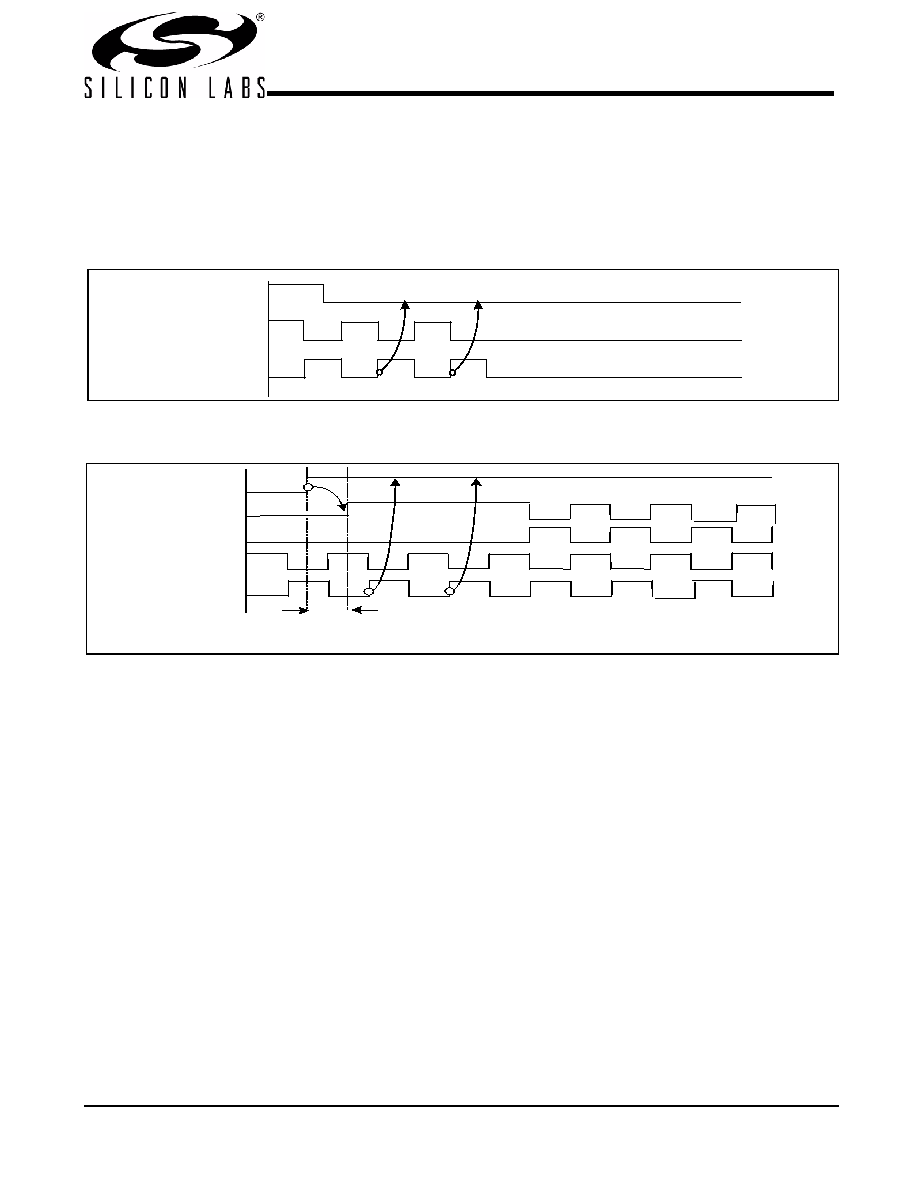
CPU_STP# Clarification
The CPU_STP# signal is an active LOW input used for cleanly
stopping and starting the CPU outputs while the rest of the
clock generator continues to function. Note that the assertion
and deassertion of this signal is absolutely asynchronous.
CPU_STP# Assertion
The CPU_STP# signal is an active LOW input used for
synchronous stopping and starting of the CPU output clocks
while the rest of the clock generator continues to function.
When the CPU_STP# pin is asserted, all CPU outputs that are
set with the SMBus configuration to be stoppable via assertion
of CPU_STP# will be stopped after being sampled by 2 to 6
rising edges of the internal CPUC clock. The final state of the
stopped CPU clock is LOW due to tri-state; both CPUT and
CPUC outputs will not be driven.
CPU_STP# Deassertion
The deassertion of the CPU_STP# signal will cause all CPU
outputs that were stopped to resume normal operation in a
synchronous manner, synchronous manner meaning that no
short or stretched clock pulses will be produced when the
clock resumes. The maximum latency from the deassertion to
active outputs is between 2 and 6 CPU clock periods (2 clocks
are shown). If the control register tri-state bit corresponding to
the output of interest is programmed to '1', then the stopped
CPU outputs will be driven HIGH within 10 ns of CPU_Stop#
deassertion to a voltage greater than 200 mV.
PCI_STP# Clarification
The PCI_STP# signal is an active LOW input used for cleanly
stopping and starting the PCI and PCIEX outputs while the rest
of the clock generator continues to function. The PCIF and
PCIEX clocks are special in that they can be programmed to
ignore PCI_STP# by setting the register bit corresponding to
the output of interest to free running. Outputs set to free
running will ignore the PCI_STP# pin.
PCI_STP# Assertion
The impact of asserting the PCI_STP# signal is as follows. The
clock chip is to sample the PCI_STP# signal on a rising edge
of PCIF clock. After detecting the PCI_STP# assertion LOW,
all PCI and stoppable PCIF clocks will latch LOW on their next
HIGH-to-LOW transition. After the PCI clocks are latched
LOW, the stoppable PCIEX clocks will latch to LOW due to
tri-state, as shown in Figure 7. The one PCI clock latency
shown is critical to system functionality; any violation of this
may result in system failure. The Tsu_pci_stp# is the setup
time required by the clock generator to correctly sample the
PCI_STP# assertion. This time is 10 ns minimum.
PCI_STP# Deassertion
The deassertion of the PCI_STP# signal functions as follows.
The deassertion of the PCI_STP# signal is to be sampled on
the rising edge of the PCIF free running clock domain. After
detecting PCI_STP# deassertion, all PCI, stoppable PCIF and
stoppable PCIEX clocks will resume in a glitch-free manner.
The PCI and PCIEX clock resume latency should exactly
match the 1 PCI clock latency required for PCI_STP# entry.
The stoppable PCIEX clocks must be driven HIGH within
15 ns of PCI_STP# deassertion. Figure 8 shows the appro-
priate relationship. The Tsu_cpu_stp# is the setup time
required by the clock generator to correctly sample the
PCI_STP# deassertion. This time is 10 ns minimum.
CPU_STP#
CPUT
CPUC
Figure 5. CPU_STP# Assertion Timing Waveform
CP U _ S T P #
CP UT
CP UC
CP U T In t e r n a l
T d r iv e _ C P U _ S T P #, 10 n S > 200 m V
CP UC In t e r n a l
Figure 6. CPU_STP# Deassertion
相关PDF资料 |
PDF描述 |
|---|---|
| CY2SSTV855ZXI | IC CLOCK DIFFDRV PLL DDR 28TSSOP |
| CY2SSTV857ZXI-27 | IC CLK DDR266/333BUF1:10 48TSSOP |
| CY2SSTV857ZXI-32 | IC CLK DDR266/333BUF1:10 48TSSOP |
| CY505YC64DT | IC CLK CK505 BROADWATER 64TSSOP |
| CYW150OXC | IC CLOCK 440BX AGP 56SSOP |
相关代理商/技术参数 |
参数描述 |
|---|---|
| CY28551LFXC-3 | 功能描述:时钟发生器及支持产品 Universal System Clk Intel AMD SiS Via RoHS:否 制造商:Silicon Labs 类型:Clock Generators 最大输入频率:14.318 MHz 最大输出频率:166 MHz 输出端数量:16 占空比 - 最大:55 % 工作电源电压:3.3 V 工作电源电流:1 mA 最大工作温度:+ 85 C 安装风格:SMD/SMT 封装 / 箱体:QFN-56 |
| CY28551LFXC-3T | 功能描述:时钟发生器及支持产品 Universal System Clk Intel AMD SiS Via RoHS:否 制造商:Silicon Labs 类型:Clock Generators 最大输入频率:14.318 MHz 最大输出频率:166 MHz 输出端数量:16 占空比 - 最大:55 % 工作电源电压:3.3 V 工作电源电流:1 mA 最大工作温度:+ 85 C 安装风格:SMD/SMT 封装 / 箱体:QFN-56 |
| CY28551LFXCT | 功能描述:时钟发生器及支持产品 Universal System Clk Intel AMD SiS Via RoHS:否 制造商:Silicon Labs 类型:Clock Generators 最大输入频率:14.318 MHz 最大输出频率:166 MHz 输出端数量:16 占空比 - 最大:55 % 工作电源电压:3.3 V 工作电源电流:1 mA 最大工作温度:+ 85 C 安装风格:SMD/SMT 封装 / 箱体:QFN-56 |
| CY2862-000 | 制造商:TE Connectivity 功能描述:82A0111-4-9-G110 |
| CY2863-000 | 制造商:TE Connectivity 功能描述:82A0111-8-9-G110 - Bulk |
发布紧急采购,3分钟左右您将得到回复。