- 您现在的位置:买卖IC网 > PDF目录9593 > CY2SSTV857ZXC-27T (Silicon Laboratories Inc)IC CLK DDR266/333BUF1:10 48TSSOP PDF资料下载
参数资料
| 型号: | CY2SSTV857ZXC-27T |
| 厂商: | Silicon Laboratories Inc |
| 文件页数: | 2/8页 |
| 文件大小: | 0K |
| 描述: | IC CLK DDR266/333BUF1:10 48TSSOP |
| 标准包装: | 2,000 |
| 系列: | * |
| 类型: | * |
| PLL: | * |
| 主要目的: | * |
| 输入: | * |
| 输出: | * |
| 电路数: | * |
| 比率 - 输入:输出: | * |
| 差分 - 输入:输出: | * |
| 频率 - 最大: | * |
| 电源电压: | * |
| 工作温度: | * |
| 安装类型: | * |
| 封装/外壳: | * |
| 供应商设备封装: | * |
| 包装: | * |
CY2SSTV857
.......................... Document #: 38-07464 Rev. *F Page 2 of 8
Zero-delay Buffer
When used as a zero-delay buffer the CY2SSTV857-27 will
likely be in a nested clock tree application. For these applica-
tions the CY2SSTV857-27 offers a differential clock input pair
as a PLL reference. The CY2SSTV857-27 then can lock onto
the reference and translate with near-zero delay to low-skew
outputs. For normal operation, the external feedback input,
FBIN, is connected to the feedback output, FBOUT. By
connecting the feedback output to the feedback input the
propagation delay through the device is eliminated. The PLL
works to align the output edge with the input reference edge
thus producing a near-zero delay. The reference frequency
affects the static phase offset of the PLL and thus the relative
delay between the inputs and outputs.
When VDDA is strapped LOW, the PLL is turned off and
bypassed for test purposes.
Power Management
Output enable/disable control of the CY2SSTV857-27 allows
the user to implement power management schemes into the
design. Outputs are three-stated/disabled when PD# is
asserted low (see Table 1).
Note:
1. A bypass capacitor (0.1
F) should be placed as close as possible to each positive power pin (<0.2”). If these bypass capacitors are not close to the pins, their
high-frequency filtering characteristic will be cancelled by the lead inductance of the traces.
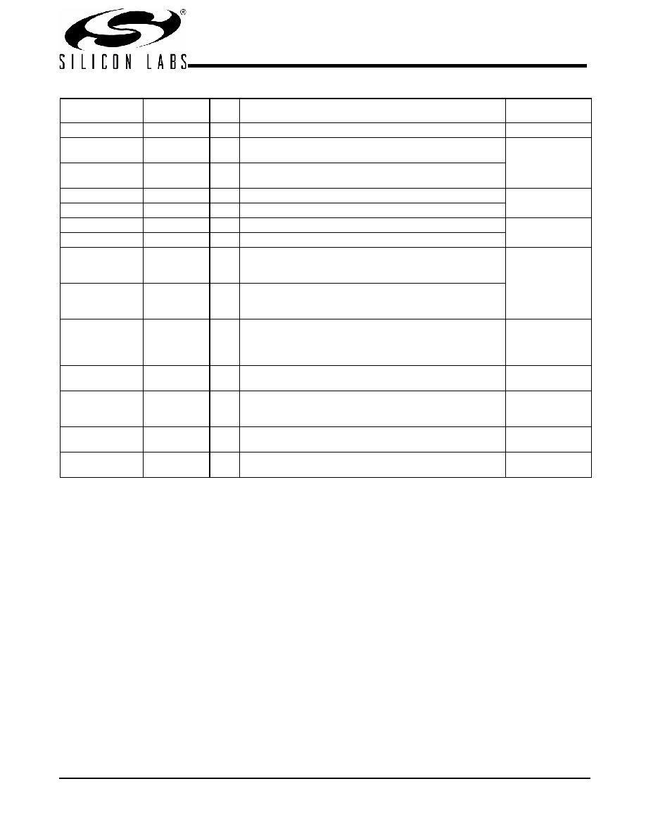
Pin Description
Pin Number
Pin Name
I/O[1]
Pin Description
Electrical
Characteristics
13, 14
CLK, CLK#
I
Differential Clock Input.
LV Differential Input
35
FBIN#
I
Feedback Clock Input. Connect to FBOUT# for accessing the
PLL.
Differential Input
36
FBIN
I
Feedback Clock Input. Connect to FBOUT for accessing the
PLL.
3, 5, 10, 20, 22
Y(0:4)
O
Clock Outputs
Differential Outputs
2, 6, 9, 19, 23
Y#(0:4)
O
Clock Outputs
27, 29, 39, 44, 46
Y(9:5)
O
Clock Outputs
Differential Outputs
26, 30, 40, 43, 47
Y#(9:5)
O
Clock Outputs
32
FBOUT
O
Feedback Clock Output. Connect to FBIN for normal
operation. A bypass delay capacitor at this output will control
Input Reference/Output Clocks phase relationships.
Differential Outputs
33
FBOUT#
O
Feedback Clock Output. Connect to FBIN# for normal
operation. A bypass delay capacitor at this output will control
Input Reference/Output Clocks phase relationships.
37
PD#
I
Power Down# Input. When PD# is set HIGH, all Q and Q#
outputs are enabled and switch at the same frequency as CLK.
When set LOW, all Q and Q# outputs are disabled Hi-Z and the
PLL is powered down.
4, 11,12,15, 21, 28,
34, 38, 45
VDDQ
2.5V Power Supply for Output Clock Buffers.2.5V Nominal
16
AVDD
2.5V Power Supply for PLL. When VDDA is at GND, PLL is
bypassed and CLK is buffered directly to the device outputs.
During disable (PD# = 0), the PLL is powered down.
2.5V Nominal
1, 7, 8, 18, 24, 25,
31, 41, 42, 48
VSS
Common Ground
0.0V Ground
17
AVSS
Analog Ground
0.0V Analog
Ground
相关PDF资料 |
PDF描述 |
|---|---|
| VE-23K-MX-F4 | CONVERTER MOD DC/DC 40V 75W |
| VI-214-MX-F2 | CONVERTER MOD DC/DC 48V 75W |
| ISL8483IB-T | TRANSCEIVER RS-485/422 5V 8-SOIC |
| MS3451L20-7S | CONN RCPT 8POS CBL MNT W/SCKT |
| VI-213-MX-F4 | CONVERTER MOD DC/DC 24V 75W |
相关代理商/技术参数 |
参数描述 |
|---|---|
| CY2SSTV857ZXC-32 | 功能描述:时钟缓冲器 2.5V 60-200MHz 1:10 Diff DDR266/333 B/D RoHS:否 制造商:Texas Instruments 输出端数量:5 最大输入频率:40 MHz 传播延迟(最大值): 电源电压-最大:3.45 V 电源电压-最小:2.375 V 最大功率耗散: 最大工作温度:+ 85 C 最小工作温度:- 40 C 封装 / 箱体:LLP-24 封装:Reel |
| CY2SSTV857ZXC-32T | 功能描述:时钟缓冲器 2.5V 60-200MHz 1:10 Diff DDR266/333 B/D RoHS:否 制造商:Texas Instruments 输出端数量:5 最大输入频率:40 MHz 传播延迟(最大值): 电源电压-最大:3.45 V 电源电压-最小:2.375 V 最大功率耗散: 最大工作温度:+ 85 C 最小工作温度:- 40 C 封装 / 箱体:LLP-24 封装:Reel |
| CY2SSTV857ZXI-27 | 功能描述:时钟缓冲器 2.5V 60-200MHz 1:10 Diff DDR266/333 B/D RoHS:否 制造商:Texas Instruments 输出端数量:5 最大输入频率:40 MHz 传播延迟(最大值): 电源电压-最大:3.45 V 电源电压-最小:2.375 V 最大功率耗散: 最大工作温度:+ 85 C 最小工作温度:- 40 C 封装 / 箱体:LLP-24 封装:Reel |
| CY2SSTV857ZXI-27T | 功能描述:时钟缓冲器 2.5V 60-200MHz 1:10 Diff DDR266/333 B/D RoHS:否 制造商:Texas Instruments 输出端数量:5 最大输入频率:40 MHz 传播延迟(最大值): 电源电压-最大:3.45 V 电源电压-最小:2.375 V 最大功率耗散: 最大工作温度:+ 85 C 最小工作温度:- 40 C 封装 / 箱体:LLP-24 封装:Reel |
| CY2SSTV857ZXI-32 | 功能描述:时钟缓冲器 2.5V 60-200MHz 1:10 Diff DDR266/333 B/D RoHS:否 制造商:Texas Instruments 输出端数量:5 最大输入频率:40 MHz 传播延迟(最大值): 电源电压-最大:3.45 V 电源电压-最小:2.375 V 最大功率耗散: 最大工作温度:+ 85 C 最小工作温度:- 40 C 封装 / 箱体:LLP-24 封装:Reel |
发布紧急采购,3分钟左右您将得到回复。