- 您现在的位置:买卖IC网 > PDF目录170346 > CY39050Z208-222NC (CYPRESS SEMICONDUCTOR CORP) LOADABLE PLD, 7 ns, PQFP208 PDF资料下载
参数资料
| 型号: | CY39050Z208-222NC |
| 厂商: | CYPRESS SEMICONDUCTOR CORP |
| 元件分类: | PLD |
| 英文描述: | LOADABLE PLD, 7 ns, PQFP208 |
| 封装: | PLASTIC, QFP-208 |
| 文件页数: | 15/57页 |
| 文件大小: | 1166K |
| 代理商: | CY39050Z208-222NC |
第1页第2页第3页第4页第5页第6页第7页第8页第9页第10页第11页第12页第13页第14页当前第15页第16页第17页第18页第19页第20页第21页第22页第23页第24页第25页第26页第27页第28页第29页第30页第31页第32页第33页第34页第35页第36页第37页第38页第39页第40页第41页第42页第43页第44页第45页第46页第47页第48页第49页第50页第51页第52页第53页第54页第55页第56页第57页
PRELIMINARY
Delta39K ISR
CPLD Family
Document #: 38-03039 Rev. **
Page 22 of 57
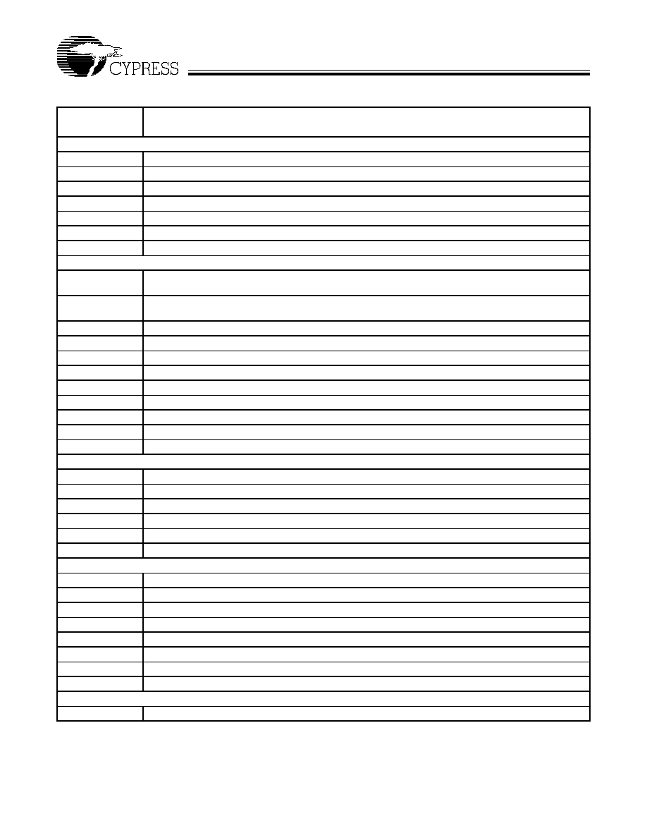
Channel Memory Timing Parameter Descriptions Over the Operating Range
Parameter
Description
Dual Port Asynchronous Mode Parameters
tCHMAA
Channel memory access time. Delay from address change to read data out
tCHMPWE
Write enable pulse width
tCHMSA
Address set-up to the beginning of write enable with both signals from the same I/O block
tCHMHA
Address hold after the end of write enable with both signals from the same I/O block
tCHMSD
Data set-up to the end of write enable
tCHMHD
Data hold after the end of write enable
tCHMBA
Channel memory asynchronous dual port address match (busy access time)
Dual Port Synchronous Mode Parameters
tCHMCYC1
Clock cycle time for flow through read and write operations (from macrocell register through channel
memory back to a macrocell register in the same cluster)
tCHMCYC2
Clock cycle time for pipelined read and write operations (from channel memory input register through the
memory to channel memory output register)
tCHMS
Address, data, and WE set-up time of pin inputs, relative to a global clock
tCHMH
Address, data, and WE hold time of pin inputs, relative to a global clock
tCHMDV1
Global clock to data valid on output pins for flow through data
tCHMDV2
Global clock to data valid on output pins for pipelined data.
tCHMBDV
Channel memory synchronous dual-port address match (busy, clock to data valid)
tCHMMACS1
Channel memory input clock to macrocell clock in the same cluster
tCHMMACS2
Channel memory output clock to macrocell clock in the same cluster
tMACCHMS1
Macrocell clock to channel memory input clock in the same cluster
tMACCHMS2
Macrocell clock to channel memory output clock in the same cluster
Synchronous FIFO Data Parameters
tCHMCLK
Read and write minimum clock cycle time
tCHMFS
Data, read enable, and write enable set-up time relative to pin inputs
tCHMFH
Data, read enable, and write enable hold time relative to pin inputs
tCHMFRDV
Data access time to output pins from rising edge of read clock (read clock to data valid)
tCHMMACS
Channel memory FIFO read clock to macrocell clock for read data
tMACCHMS
Macrocell clock to channel memory FIFO write clock for write data
Synchronous FIFO Flag Parameters
tCHMFO
Read or write clock to respective flag output at output pins
tCHMMACF
Read or write clock to macrocell clock with FIFO flag
tCHMFRS
Master Reset Pulse Width
tCHMFRSR
Master Reset Recovery Time
tCHMFRSF
Master Reset to Flag and Data Output Time
tCHMSKEW1
Read/Write Clock Skew Time for Full Flag
tCHMSKEW2
Read/Write Clock Skew Time for Empty Flag
tCHMSKEW3
Read/Write Clock Skew Time for Boundary Flags
Internal Parameters
tCHMCHAA
Asynchronous channel memory access time from input of channel memory to output of channel memory
相关PDF资料 |
PDF描述 |
|---|---|
| CY39050Z256-222BBC | LOADABLE PLD, 7 ns, PBGA256 |
| CY39050Z388-222MGC | LOADABLE PLD, 7 ns, PBGA388 |
| CY39050Z484-222MBC | LOADABLE PLD, 7 ns, PBGA484 |
| CY39200V208-167NTC | LOADABLE PLD, 8.5 ns, PQFP208 |
| CY39200V388-167MGC | LOADABLE PLD, 8.5 ns, PBGA388 |
相关代理商/技术参数 |
参数描述 |
|---|---|
| CY39050Z388-125BBC | 制造商:CYPRESS 制造商全称:Cypress Semiconductor 功能描述:CPLDs at FPGA Densities |
| CY39050Z388-125BBI | 制造商:CYPRESS 制造商全称:Cypress Semiconductor 功能描述:CPLDs at FPGA Densities |
| CY39050Z484-125BBC | 制造商:CYPRESS 制造商全称:Cypress Semiconductor 功能描述:CPLDs at FPGA Densities |
| CY39050Z484-125BBI | 制造商:CYPRESS 制造商全称:Cypress Semiconductor 功能描述:CPLDs at FPGA Densities |
| CY39050Z676-125BBC | 制造商:CYPRESS 制造商全称:Cypress Semiconductor 功能描述:CPLDs at FPGA Densities |
发布紧急采购,3分钟左右您将得到回复。