- 您现在的位置:买卖IC网 > PDF目录170346 > CY39050Z208-222NC (CYPRESS SEMICONDUCTOR CORP) LOADABLE PLD, 7 ns, PQFP208 PDF资料下载
参数资料
| 型号: | CY39050Z208-222NC |
| 厂商: | CYPRESS SEMICONDUCTOR CORP |
| 元件分类: | PLD |
| 英文描述: | LOADABLE PLD, 7 ns, PQFP208 |
| 封装: | PLASTIC, QFP-208 |
| 文件页数: | 56/57页 |
| 文件大小: | 1166K |
| 代理商: | CY39050Z208-222NC |
第1页第2页第3页第4页第5页第6页第7页第8页第9页第10页第11页第12页第13页第14页第15页第16页第17页第18页第19页第20页第21页第22页第23页第24页第25页第26页第27页第28页第29页第30页第31页第32页第33页第34页第35页第36页第37页第38页第39页第40页第41页第42页第43页第44页第45页第46页第47页第48页第49页第50页第51页第52页第53页第54页第55页当前第56页第57页
PRELIMINARY
Delta39K ISR
CPLD Family
Document #: 38-03039 Rev. **
Page 8 of 57
The clocks for each port of the Dual-Port configuration are
selected from four global clocks and two local clocks. One lo-
cal clock is sourced from the horizontal channel and the other
from the vertical channel. The data outputs of the dual-port
memory can also be registered. Clocks for the output registers
are also selected from four global clocks and two local clocks.
One clock polarity mux per port allows the use of true or com-
plement polarity for input and output clocking purposes.
Arbitration
The Dual-Port configuration of the Channel Memory Block pro-
vides arbitration when both ports access the same address at
the same time. Depending on the memory operation being at-
tempted, one port always gets priority. See Table 1 for details
on which port gets priority for read and write operations. An
active-LOW ‘Address Match’ signal is generated when an ad-
dress collision occurs.
FIFO (Channel Memory) Configuration
The channel memory blocks are also configurable as synchro-
nous FIFO RAM. In the FIFO mode of operation, the channel
memory block supports all normal FIFO operations without the
use of any general-purpose logic resources in the device.
The FIFO block contains all of the necessary FIFO flag logic,
including the read and write address pointers. The FIFO flags
include an empty/full flag (EF), half-full flag (HF), and program-
mable almost-empty/full (PAEF) flag output. The FIFO config-
uration has the ability to perform simultaneous read and write
operations using two separate clocks. These clocks may be
tied together for a single operation or may run independently
for asynchronous Read/Write (w.r.t. each other) applications.
The data and control inputs to the FIFO block are driven from
the horizontal or vertical routing channels. The data and flag
outputs are driven onto dedicated routing tracks in both the
horizontal and vertical routing channels. This allows the FIFO
blocks to be expanded by using multiple FIFO blocks on the
same horizontal or vertical routing channel without any speed
penalty.
In FIFO mode, the write and read ports are controlled by sep-
arate clock and enable signals. The clocks for each port are
selected from four global clocks and two local clocks.
One local clock is sourced from the horizontal channel and the
other from the vertical channel. The data outputs from the read
port of the FIFO can also be registered. One clock polarity mux
per port allows using true or complement polarity for read and
write operations. The write operation is controlled by the clock
and the write enable pin. The read operation is controlled by
the clock and the read enable pin. The enable pins can be
sourced from horizontal or vertical channels.
Table 1. Arbitration Result: Address Match Signal
Becomes Active
Port A
Port B
Result of
Arbitration
Comment
Read
No arbitration
required
Both ports read at the
same time
Write
Read
Port A gets
priority
If Port B requests first
then it will read the cur-
rent data. The output will
then change to the newly
written data by Port A
Read
Write
Port B gets
priority
If Port A requests first
then it will read the cur-
rent data. The output will
then change to the newly
written data by Port B
Write
Port A gets
priority
Port B is blocked until
Port A is finished writing
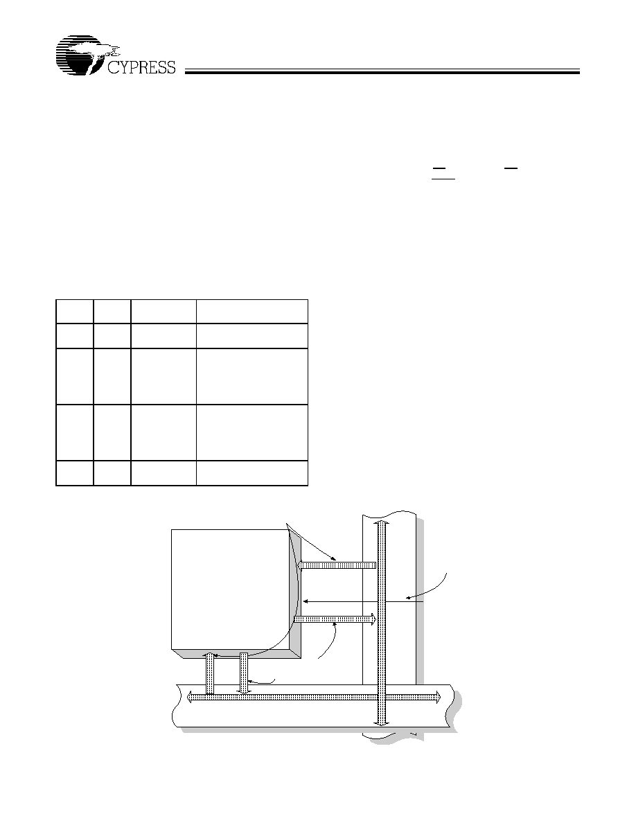
Figure 6. Block Diagram of Channel Memory Block
4096-bit Dual Port
Array
Configurable as
Async/Sync Dual Port or
Sync FIFO
Configurable as
4Kx1, 2Kx2, 1Kx4 and
512x8 block sizes
Horizontal Channel
All channel memory
inputs are driven from
the routing channels
All channel memory outputs
drive dedicated tracks in the
routing channels
GCLK[3:0]
Global Clock
Signals
Ver
tic
al
C
hannel
相关PDF资料 |
PDF描述 |
|---|---|
| CY39050Z256-222BBC | LOADABLE PLD, 7 ns, PBGA256 |
| CY39050Z388-222MGC | LOADABLE PLD, 7 ns, PBGA388 |
| CY39050Z484-222MBC | LOADABLE PLD, 7 ns, PBGA484 |
| CY39200V208-167NTC | LOADABLE PLD, 8.5 ns, PQFP208 |
| CY39200V388-167MGC | LOADABLE PLD, 8.5 ns, PBGA388 |
相关代理商/技术参数 |
参数描述 |
|---|---|
| CY39050Z388-125BBC | 制造商:CYPRESS 制造商全称:Cypress Semiconductor 功能描述:CPLDs at FPGA Densities |
| CY39050Z388-125BBI | 制造商:CYPRESS 制造商全称:Cypress Semiconductor 功能描述:CPLDs at FPGA Densities |
| CY39050Z484-125BBC | 制造商:CYPRESS 制造商全称:Cypress Semiconductor 功能描述:CPLDs at FPGA Densities |
| CY39050Z484-125BBI | 制造商:CYPRESS 制造商全称:Cypress Semiconductor 功能描述:CPLDs at FPGA Densities |
| CY39050Z676-125BBC | 制造商:CYPRESS 制造商全称:Cypress Semiconductor 功能描述:CPLDs at FPGA Densities |
发布紧急采购,3分钟左右您将得到回复。