- 您现在的位置:买卖IC网 > PDF目录380137 > CY39200V388-233NC (Cypress Semiconductor Corp.) CPLDs at FPGA Densities PDF资料下载
参数资料
| 型号: | CY39200V388-233NC |
| 厂商: | Cypress Semiconductor Corp. |
| 英文描述: | CPLDs at FPGA Densities |
| 中文描述: | CPLD器件在FPGA的密度 |
| 文件页数: | 7/86页 |
| 文件大小: | 1235K |
| 代理商: | CY39200V388-233NC |
第1页第2页第3页第4页第5页第6页当前第7页第8页第9页第10页第11页第12页第13页第14页第15页第16页第17页第18页第19页第20页第21页第22页第23页第24页第25页第26页第27页第28页第29页第30页第31页第32页第33页第34页第35页第36页第37页第38页第39页第40页第41页第42页第43页第44页第45页第46页第47页第48页第49页第50页第51页第52页第53页第54页第55页第56页第57页第58页第59页第60页第61页第62页第63页第64页第65页第66页第67页第68页第69页第70页第71页第72页第73页第74页第75页第76页第77页第78页第79页第80页第81页第82页第83页第84页第85页第86页
Delta39K ISR
CPLD Family
Document #: 38-03039 Rev. *H
Page 7 of 86
Embedded Memory
Each member of the Delta39K family contains two types of
embedded memory blocks. The channel memory block is
placed at the intersection of horizontal and vertical routing
channels. Each channel memory block is 4096 bits in size and
can be configured as asynchronous or synchronous Dual-Port
RAM, Single-Port RAM, Read-Only memory (ROM), or
synchronous FIFO memory. The memory organization is
configurable as 4K × 1, 2K × 2, 1K × 4 and 512K × 8. The
second type of memory block is located within each LBC and
is referred to as a cluster memory block. Each LBC contains
two cluster memory blocks that are 8192 bits in size. Similar
to the channel memory blocks, the cluster memory blocks can
be configured as 8K × 1, 4K × 2, 2K × 4 and 1K × 8
asynchronous or synchronous Single-Port RAM or ROM.
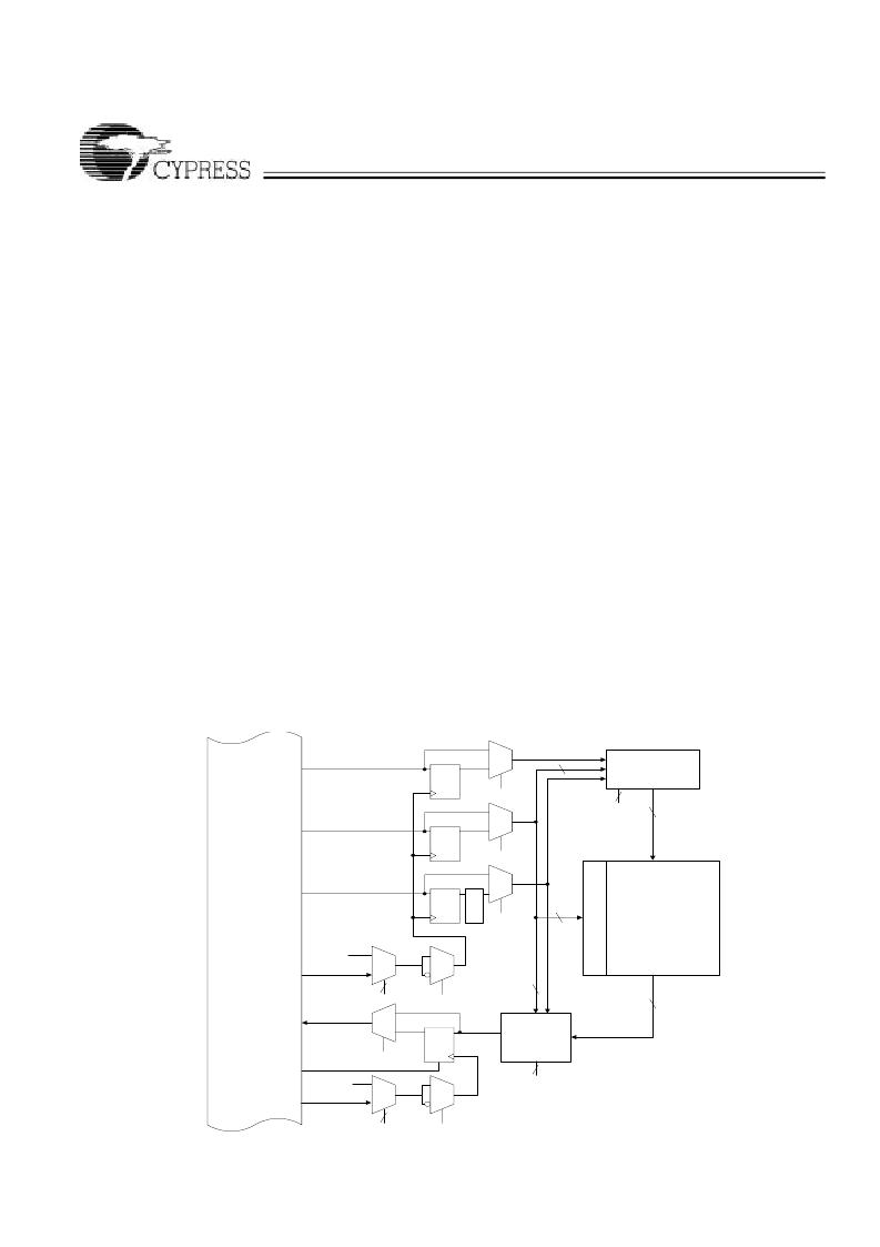
Cluster Memory
Each logic block cluster of the Delta39K contains two 8192-bit
cluster memory blocks.
Figure 5
is a block diagram of the
cluster memory block and the interface of the cluster memory
block to the cluster PIM.
The output of the cluster memory block can be optionally regis-
tered to perform synchronous pipelining or to register
asynchronous Read and Write operations. The output
registers contain an asynchronous RESET which can be used
in any type of sequential logic circuits (e.g., state machines).
There are four global clocks (GCLK[3:0]) and one local clock
available for the input and the output registers. The local clock
for the input registers is independent of the one used for the
output registers. The local clock is generated in the user
design in a macrocell or comes from an I/O pin.
Cluster Memory Initialization
The cluster memory powers up in an undefined state, but is set
to a user-defined known state during configuration. To facilitate
the use of look-up-table (LUT) logic and ROM applications, the
cluster memory blocks can be initialized with a given set of
data when the device is configured at power up. For LUT and
ROM applications, the user cannot write to memory blocks.
Channel Memory
The Delta39K architecture includes an embedded memory
block at each crossing point of horizontal and vertical routing
channels. The channel memory is a 4096-bit embedded
memory block that can be configured as asynchronous or
synchronous single-port RAM, dual-port RAM, ROM, or
synchronous FIFO memory.
Data, address, and control inputs to the channel memory are
driven from horizontal and vertical routing channels. All data
and FIFO logic outputs drive dedicated tracks in the horizontal
and vertical routing channels. The clocks for the channel
memory block are selected from four global clocks and pin
inputs from the horizontal and vertical channels. The clock
muxes also include a polarity mux for each clock so that the
user can choose an inverted clock.
Dual-Port (Channel Memory) Configuration
Each port has distinct address inputs, as well as separate data
and control inputs that can be accessed simultaneously. The
inputs to the Dual-Port memory are driven from the horizontal
and vertical routing channels. The data outputs drive
dedicated tracks in the routing channels. The interface to the
routing is such that Port A of the Dual-Port interfaces primarily
with the horizontal routing channel and Port B interfaces
primarily with the vertical routing channel.
5:1
DIN[7:0]
D Q
ADDR[12:0]
D Q
Cluster PIM
D Q
WE
W
P
Write
Logic
As1024x8
SRAM
Read
Logic
R
DOUT[7:0]
8
3
3
8
10
C
C
D
Q
GCLK[3:0]
Local CLK
5:1
R
RESET
GCLK[3:0]
C
2
Local CLK
3
2
3
C
C
C
C
C
C
C
Figure 5. Block Diagram of Cluster Memory Block
相关PDF资料 |
PDF描述 |
|---|---|
| CY39200V388-233NI | CPLDs at FPGA Densities |
| CY39200V388-233NTI | CPLDs at FPGA Densities |
| CY39200V388-83BBC | CPLDs at FPGA Densities |
| CY39200V388-83BBI | CPLDs at FPGA Densities |
| CY39200V388-83BGC | CPLDs at FPGA Densities |
相关代理商/技术参数 |
参数描述 |
|---|---|
| CY39200V388-233NTC | 制造商:CYPRESS 制造商全称:Cypress Semiconductor 功能描述:CPLDs at FPGA Densities |
| CY39200V388-83MGC | 制造商:Cypress Semiconductor 功能描述: |
| CY39200V484-125BBC | 制造商:CYPRESS 制造商全称:Cypress Semiconductor 功能描述:CPLDs at FPGA Densities |
| CY39200V484-125BBI | 制造商:CYPRESS 制造商全称:Cypress Semiconductor 功能描述:CPLDs at FPGA Densities |
| CY39200V484-125BBXC | 功能描述:CPLD - 复杂可编程逻辑器件 Delta39K 200K 125MHz COM RoHS:否 制造商:Lattice 系列: 存储类型:EEPROM 大电池数量:128 最大工作频率:333 MHz 延迟时间:2.7 ns 可编程输入/输出端数量:64 工作电源电压:3.3 V 最大工作温度:+ 90 C 最小工作温度:0 C 封装 / 箱体:TQFP-100 |
发布紧急采购,3分钟左右您将得到回复。