- 您现在的位置:买卖IC网 > PDF目录295354 > CY7C0851AV-133AXI (CYPRESS SEMICONDUCTOR CORP) FLEx36™ 3.3V 32K/64K/128K/256K x 36 Synchronous Dual-Port RAM PDF资料下载
参数资料
| 型号: | CY7C0851AV-133AXI |
| 厂商: | CYPRESS SEMICONDUCTOR CORP |
| 元件分类: | SRAM |
| 英文描述: | FLEx36™ 3.3V 32K/64K/128K/256K x 36 Synchronous Dual-Port RAM |
| 中文描述: | 64K X 36 DUAL-PORT SRAM, 4 ns, PQFP176 |
| 封装: | 24 X 24 MM, 1.40 MM HEIGHT, LEAD FREE, TQFP-176 |
| 文件页数: | 35/36页 |
| 文件大小: | 956K |
| 代理商: | CY7C0851AV-133AXI |
第1页第2页第3页第4页第5页第6页第7页第8页第9页第10页第11页第12页第13页第14页第15页第16页第17页第18页第19页第20页第21页第22页第23页第24页第25页第26页第27页第28页第29页第30页第31页第32页第33页第34页当前第35页第36页
CY7C0850AV,CY7C0851V/CY7C0851AV
CY7C0852V/CY7C0852AV
CY7C0853V/CY7C0853AV
Document #: 38-06070 Rev. *J
Page 8 of 36
Master Reset
The FLEx36 family devices undergo a complete reset by taking
its MRST input LOW. The MRST input can switch
asynchronously to the clocks. The MRST initializes the internal
burst counters to zero, and the counter mask registers to all ones
(completely unmasked). The MRST also forces the Mailbox
Interrupt (INT) flags and the Counter Interrupt (CNTINT) flags
HIGH. The MRST must be performed on the FLEx36 family
devices after power up.
Mailbox Interrupts
The upper two memory locations may be used for message
passing and permit communications between ports. Table 2
shows
the
interrupt
operation
for
both
ports
of
CY7C853V/CY7C0853AV. The highest memory location, 3FFFF
is the mailbox for the right port and 3FFFE is the mailbox for the
operation by the left port to address 3FFFF asserts INTR LOW.
At least one byte has to be active for a Write to generate an
interrupt. A valid Read of the 3FFFF location by the right port
resets INTR HIGH. At least one byte has to be active in order for
a Read to reset the interrupt. When one port Writes to the other
port’s mailbox, the INT of the port that the mailbox belongs to is
asserted LOW. The INT is reset when the owner (port) of the
mailbox Reads the contents of the mailbox. The interrupt flag is
set in a flow-thru mode (that is it follows the clock edge of the
writing port). Also, the flag is reset in a flow-thru mode (that is it
follows the clock edge of the reading port).
Each port can read the other port’s mailbox without resetting the
interrupt. And each port can write to its own mailbox without
setting the interrupt. If an application does not require message
passing, INT pins should be left open.
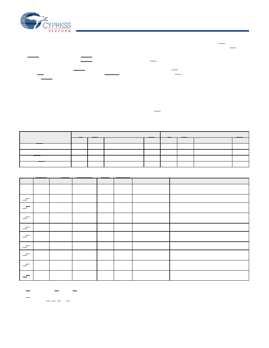
Table 2. Interrupt Operation Example [5, 6, 7, 8, 9]
Function
Left Port
Right Port
R/WL
CEL
A0L–17L
INTL
R/WR
CER
A0R–17R
INTR
Set right INTR flag
L
3FFFF
X
L
Reset right INTR flag
X
H
L
3FFFF
H
Set left INTL flag
X
L
3FFFE
X
Reset left INTL flag
H
L
3FFFE
H
X
Table 3. Address Counter and Counter-Mask Register Control Operation (Any Port) [10, 11]
CLK
MRST
CNT/MSK
CNTRST
ADS
CNTEN
Operation
Description
X
L
X
Master reset
Reset address counter to all 0s and mask
register to all 1s.
H
L
X
Counter reset
Reset counter unmasked portion to all 0s.
H
L
Counter load
Load counter with external address value
presented on address lines.
H
L
H
Counter readback
Read out counter internal value on address
lines.
H
L
Counter increment
Internally increment address counter value.
H
Counter hold
Constantly hold the address value for
multiple clock cycles.
H
L
X
Mask reset
Reset mask register to all 1s.
H
L
H
L
Mask load
Load mask register with value presented on
the address lines.
H
L
H
L
H
Mask readback
Read out mask register value on address
lines.
H
L
H
X
Reserved
Operation undefined
Notes
5. 9 M device has 18 address bits, 4M device has 17 address bits, 2M device has 16 address bits, and 1M device has 15 address bits
6. CE is internal signal. CE = LOW if CE0 = LOW and CE1 = HIGH. For a single Read operation, CE only needs to be asserted once at the rising edge of the CLK and
can be deasserted after that. Data is out after the following CLK edge and is three-stated after the next CLK edge.
7. OE is “Don’t Care” for mailbox operation.
8. At least one of B0, B1, B2, or B3 must be LOW.
9. A16x is a NC for CY7C0851V/CY7C0851AV, therefore the Interrupt Addresses are FFFF and EFFF; A16x and A15x are NC for CY7C0850AV, therefore the Interrupt
Addresses are 7FFF and 6FFF.
10. “X” = “Don’t Care,” “H” = HIGH, “L” = LOW.
11. Counter operation and mask register operation is independent of chip enables.
相关PDF资料 |
PDF描述 |
|---|---|
| CY7C0851AV-133BBI | FLEx36™ 3.3V 32K/64K/128K/256K x 36 Synchronous Dual-Port RAM |
| CY7C0851AV-167BBXC | FLEx36™ 3.3V 32K/64K/128K/256K x 36 Synchronous Dual-Port RAM |
| CY7C0852AV-133AXC | FLEx36™ 3.3V 32K/64K/128K/256K x 36 Synchronous Dual-Port RAM |
| CY7C0852AV-133AXI | FLEx36™ 3.3V 32K/64K/128K/256K x 36 Synchronous Dual-Port RAM |
| CY7C0852AV-133BBI | FLEx36™ 3.3V 32K/64K/128K/256K x 36 Synchronous Dual-Port RAM |
相关代理商/技术参数 |
参数描述 |
|---|---|
| CY7C0851AV-133BBC | 制造商:Cypress Semiconductor 功能描述: 制造商:Cypress Semiconductor 功能描述:SRAM SYNC DUAL 3.3V 2.25MBIT 64KX36 4.7NS 172FBGA - Trays 制造商:Rochester Electronics LLC 功能描述: |
| CY7C0851AV-133BBI | 功能描述:静态随机存取存储器 2MB (64Kx36) 3.3v 133MHz Synch 静态随机存取存储器 RoHS:否 制造商:Cypress Semiconductor 存储容量:16 Mbit 组织:1 M x 16 访问时间:55 ns 电源电压-最大:3.6 V 电源电压-最小:2.2 V 最大工作电流:22 uA 最大工作温度:+ 85 C 最小工作温度:- 40 C 安装风格:SMD/SMT 封装 / 箱体:TSOP-48 封装:Tray |
| CY7C0851AV-167AC | 制造商:Cypress Semiconductor 功能描述:SRAM SYNC DUAL 3.3V 2.25MBIT 64KX36 4NS 176TQFP - Trays |
| CY7C0851AV-167AXC | 功能描述:静态随机存取存储器 3.3V, 64Kx36 Sync Dual Port RoHS:否 制造商:Cypress Semiconductor 存储容量:16 Mbit 组织:1 M x 16 访问时间:55 ns 电源电压-最大:3.6 V 电源电压-最小:2.2 V 最大工作电流:22 uA 最大工作温度:+ 85 C 最小工作温度:- 40 C 安装风格:SMD/SMT 封装 / 箱体:TSOP-48 封装:Tray |
| CY7C0851AV-167BBC | 制造商:Cypress Semiconductor 功能描述:SRAM SYNC DUAL 3.3V 2.25MBIT 64KX36 4NS 172FBGA - Trays 制造商:Rochester Electronics LLC 功能描述: |
发布紧急采购,3分钟左右您将得到回复。