- 您现在的位置:买卖IC网 > PDF目录378509 > CY7C1481V25-100BZXI (CYPRESS SEMICONDUCTOR CORP) 72-Mbit (2M x 36/4M x 18/1M x 72) Flow-Through SRAM PDF资料下载
参数资料
| 型号: | CY7C1481V25-100BZXI |
| 厂商: | CYPRESS SEMICONDUCTOR CORP |
| 元件分类: | DRAM |
| 英文描述: | 72-Mbit (2M x 36/4M x 18/1M x 72) Flow-Through SRAM |
| 中文描述: | 2M X 36 CACHE SRAM, 8.5 ns, PBGA165 |
| 封装: | 15 X 17 MM, 1.40 MM HEIGHT, LEAD FREE, FBGA-165 |
| 文件页数: | 14/30页 |
| 文件大小: | 1028K |
| 代理商: | CY7C1481V25-100BZXI |
第1页第2页第3页第4页第5页第6页第7页第8页第9页第10页第11页第12页第13页当前第14页第15页第16页第17页第18页第19页第20页第21页第22页第23页第24页第25页第26页第27页第28页第29页第30页
CY7C1481V25
CY7C1483V25
CY7C1487V25
Document #: 38-05281 Rev. *H
Page 14 of 30
The SRAM clock input might not be captured correctly if there
is no way in a design to stop (or slow) the clock during a
SAMPLE/PRELOAD instruction. If this is an issue, it is still
possible to capture all other signals and simply ignore the
value of the CLK captured in the boundary scan register.
Once the data is captured, it is possible to shift out the data by
putting the TAP into the Shift-DR state. This places the
boundary scan register between the TDI and TDO balls.
Note that because the PRELOAD part of the command is not
implemented, putting the TAP to the Update-DR state while
performing a SAMPLE/PRELOAD instruction has the same
effect as the Pause-DR command.
BYPASS
When the BYPASS instruction is loaded in the instruction
register and the TAP is placed in a Shift-DR state, the bypass
register is placed between the TDI and TDO balls. The
advantage of the BYPASS instruction is that it shortens the
boundary scan path when multiple devices are connected
together on a board.
Reserved
These instructions are not implemented but are reserved for
future use. Do not use these instructions.
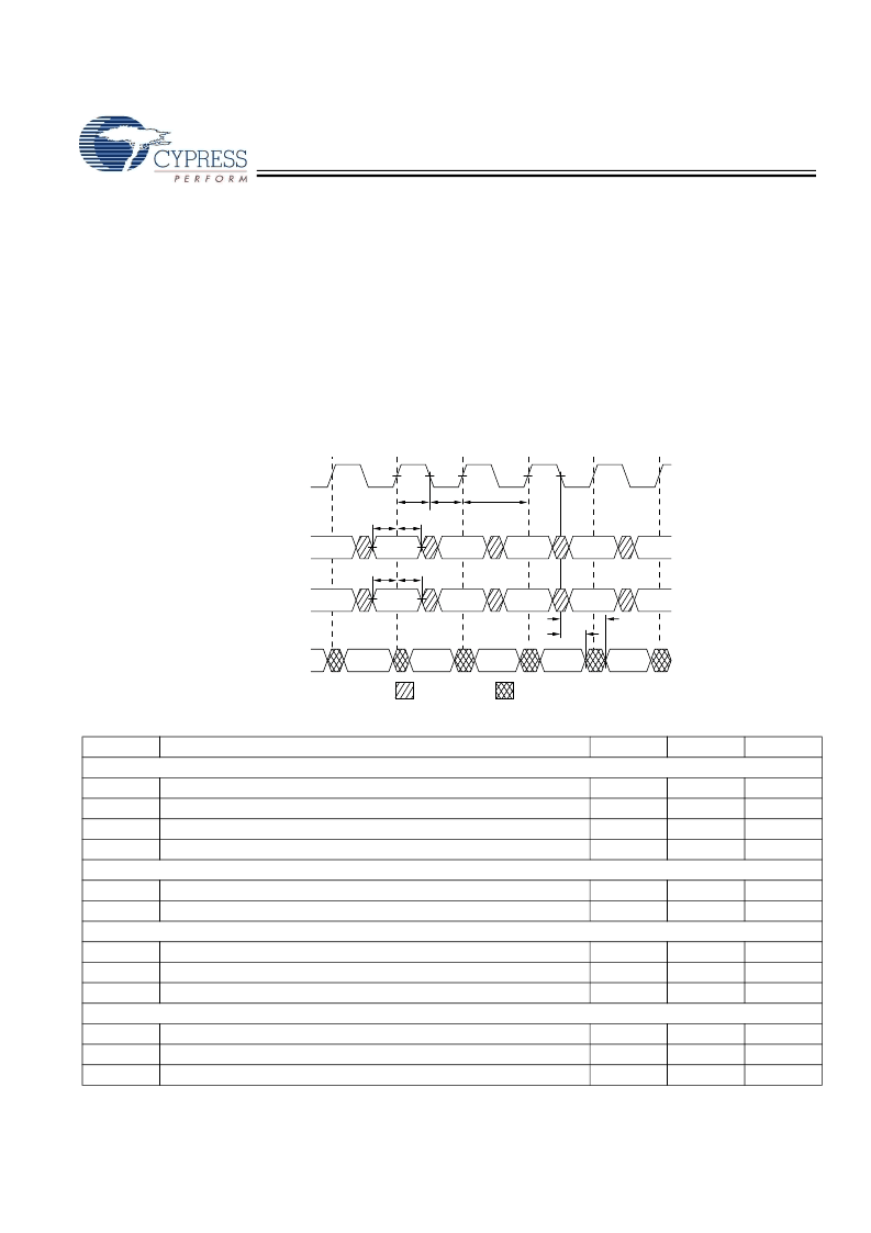
TAP Timing
TAP AC Switching Characteristics
Over the Operating Range
[10, 11]
Parameter
Clock
t
TCYC
t
TF
t
TH
t
TL
Output Times
t
TDOV
t
TDOX
Setup Times
t
TMSS
t
TDIS
t
CS
Hold Times
t
TMSH
t
TDIH
t
CH
Description
Min
Max
Unit
TCK Clock Cycle Time
TCK Clock Frequency
TCK Clock HIGH time
TCK Clock LOW time
50
ns
MHz
ns
ns
20
20
20
TCK Clock LOW to TDO Valid
TCK Clock LOW to TDO Invalid
10
ns
ns
0
TMS Setup to TCK Clock Rise
TDI Setup to TCK Clock Rise
Capture Setup to TCK Rise
5
5
5
ns
ns
TMS hold after TCK Clock Rise
TDI Hold after Clock Rise
Capture Hold after Clock Rise
5
5
5
ns
ns
ns
tTL
Test Clock
(TCK)
1
2
3
4
5
6
Test Mode Select
(TMS)
tTH
Test Data-Out
(TDO)
tCYC
Test Data-In
(TDI)
tTMSH
tTMSS
tTDIH
tTDIS
tTDOX
tTDOV
DON’T CARE
UNDEFINED
Notes
10.t
and t
refer to the setup and hold time requirements of latching data from the boundary scan register.
11. Test conditions are specified using the load in TAP AC Test Conditions. t
R
/t
F
= 1 ns.
[+] Feedback
相关PDF资料 |
PDF描述 |
|---|---|
| CY7C1481V25-133AXC | 72-Mbit (2M x 36/4M x 18/1M x 72) Flow-Through SRAM |
| CY7C1481V25-133AXI | 72-Mbit (2M x 36/4M x 18/1M x 72) Flow-Through SRAM |
| CY7C1481V25-133BZC | 72-Mbit (2M x 36/4M x 18/1M x 72) Flow-Through SRAM |
| CY7C1481V25-133BZI | 72-Mbit (2M x 36/4M x 18/1M x 72) Flow-Through SRAM |
| CY7C1481V25-133BZXC | 72-Mbit (2M x 36/4M x 18/1M x 72) Flow-Through SRAM |
相关代理商/技术参数 |
参数描述 |
|---|---|
| CY7C1481V33-100AXI | 制造商:Cypress Semiconductor 功能描述: |
| CY7C1482BV33-200BZI | 功能描述:静态随机存取存储器 72MB (4Mx18) 4.6v 200MHz 静态随机存取存储器 RoHS:否 制造商:Cypress Semiconductor 存储容量:16 Mbit 组织:1 M x 16 访问时间:55 ns 电源电压-最大:3.6 V 电源电压-最小:2.2 V 最大工作电流:22 uA 最大工作温度:+ 85 C 最小工作温度:- 40 C 安装风格:SMD/SMT 封装 / 箱体:TSOP-48 封装:Tray |
| CY7C1482BV33-250BZI | 制造商:Cypress Semiconductor 功能描述:2MX36, 3.3V SYNC PL SRAM - Bulk |
| CY7C148-35PC | 功能描述:1KX4 18-PIN POWER-DOWN SRAM RoHS:否 类别:集成电路 (IC) >> 存储器 系列:- 标准包装:1,000 系列:- 格式 - 存储器:EEPROMs - 串行 存储器类型:EEPROM 存储容量:4K (512 x 8) 速度:400kHz 接口:I²C,2 线串口 电源电压:2.7 V ~ 5.5 V 工作温度:-40°C ~ 85°C 封装/外壳:8-SOIC(0.173",4.40mm 宽) 供应商设备封装:8-MFP 包装:带卷 (TR) |
| CY7C148-45DC | 制造商:Cypress Semiconductor 功能描述:Static RAM, 1Kx4, 18 Pin, Ceramic, DIP |
发布紧急采购,3分钟左右您将得到回复。