- 您现在的位置:买卖IC网 > PDF目录223638 > CY7C343B-35JI (CYPRESS SEMICONDUCTOR CORP) OT PLD, 35 ns, PQCC44 PDF资料下载
参数资料
| 型号: | CY7C343B-35JI |
| 厂商: | CYPRESS SEMICONDUCTOR CORP |
| 元件分类: | PLD |
| 英文描述: | OT PLD, 35 ns, PQCC44 |
| 封装: | PLASTIC, LCC-44 |
| 文件页数: | 8/11页 |
| 文件大小: | 178K |
| 代理商: | CY7C343B-35JI |
CY7C343B
USE ULTRA37000TM FOR
ALL NEW DESIGNS
Document #: 38-03038 Rev. *B
Page 6 of 11
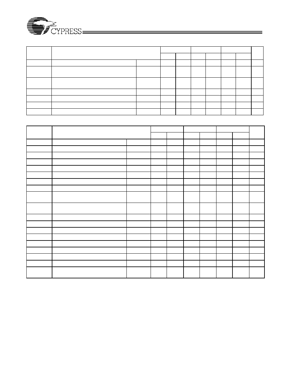
External Asynchronous Switching Characteristics Over Operating Range
Parameter
Description
7C343B-25
7C343B-30
7C343B-35
Unit
Min.
Max.
Min.
Max.
Min.
Max.
tACO1
Asynchronous Clock Input to Output Delay[4] Com’l/Ind
25
30
35
ns
tAS1
Dedicated Input or Feedback Set-Up Time to
Asynchronous Clock Input
Com’l/Ind
5
6
8ns
tAH
Input Hold Time from Asynchronous Clock
Input
Com’l/Ind
6
8
10
ns
tAWH
Asynchronous Clock Input HIGH Time[7]
Com’l/Ind
11
14
16
ns
tAWL
Asynchronous Clock Input LOW Time[7]
Com’l/Ind
9
11
14
ns
tACNT
Minimum Internal Array Clock Frequency
Com’l/Ind
20
25
30
ns
fACNT
Maximum Internal Array Clock Frequency[6] Com’l/Ind
50
40
33.3
MHz
Internal Switching Characteristics Over Operating Range
Parameter
Description
7C343B-25
7C343B-30
7C343B-35
Unit
Min.
Max.
Min.
Max.
Min.
Max.
tIN
Dedicated Input Pad and Buffer Delay Com’l/Ind
5
7
11
ns
tIO
I/O Input Pad and Buffer Delay
Com’l/Ind
6
11
ns
tEXP
Expander Array Delay
Com’l/Ind
12
14
20
ns
tLAD
Logic Array Data Delay
Com’l/Ind
12
14
ns
tLAC
Logic Array Control Delay
Com’l/Ind
10
12
13
ns
tOD
Output Buffer and Pad Delay[4]
Com’l/Ind
5
6
ns
tZX
Output Buffer Enable Delay[4]
Com’l/Ind
10
11
13
ns
tXZ
Output Buffer Disable Delay[8]
Com’l/Ind
10
11
13
ns
tRSU
Register Set-Up Time Relative to
Clock Signal at Register
Com’l/Ind
6
8
12
ns
tRH
Register Hold Time Relative to Clock
Signal at Register
Com’l/Ind
4
6
8
ns
tLATCH
Flow-Through Latch Delay
Com’l/Ind
3
4
ns
tRD
Register Delay
Com’l/Ind
1
2
ns
tCOMB
Transparent Mode Delay
Com’l/Ind
3
4
ns
tIC
Asynchronous Clock Logic Delay
Com’l/Ind
14
16
18
ns
tICS
Synchronous Clock Delay
Com’l/Ind
3
2
1
ns
tFD
Feedback Delay
Com’l/Ind
1
2
ns
tPRE
Asynchronous Register Preset Time
Com’l/Ind
5
6
7
ns
tCLR
Asynchronous Register Clear Time
Com’l/Ind
5
6
7
ns
tPIA
Programmable Interconnect Array
Delay Time
Com’l/Ind
14
16
20
ns
Notes:
7. This parameter is measured with a positive-edge-triggered clock at the register. For negative-edge clocking, the tACH and tACL parameter must be swapped.
8. C1 = 5 pF.
相关PDF资料 |
PDF描述 |
|---|---|
| CY7C343B-25HC | UV PLD, 25 ns, CQCC44 |
| CY7C343B-25HI | UV PLD, 25 ns, CQCC44 |
| CY7C343B-35HC | UV PLD, 35 ns, CQCC44 |
| CY7C343B-35HI | UV PLD, 35 ns, CQCC44 |
| CY7C344B-25JCT | OT PLD, 25 ns, PQCC28 |
相关代理商/技术参数 |
参数描述 |
|---|---|
| CY7C344-15JC | 制造商:Cypress Semiconductor 功能描述: |
| CY7C344-15PC | 制造商:Cypress Semiconductor 功能描述:CPLD MAX? Family 600 Gates 32 Macro Cells 0.8um Technology 5V 28-Pin PDIP |
| CY7C344-20JC | 制造商:Cypress Semiconductor 功能描述:CPLD MAX? Family 600 Gates 32 Macro Cells 0.8um Technology 5V 28-Pin PLCC |
| CY7C344-20JI | 制造商:Cypress Semiconductor 功能描述:CPLD MAX? Family 600 Gates 32 Macro Cells 0.8um (CMOS) Technology 5V 28-Pin PLCC 制造商:Cypress Semiconductor 功能描述:Simple EPLD, Programmable Array Logic, 28 Pin, Plastic, PLCC |
| CY7C34420WC | 制造商:CYPRESS 功能描述:* |
发布紧急采购,3分钟左右您将得到回复。