参数资料
| 型号: | CYW150OXC |
| 厂商: | Silicon Laboratories Inc |
| 文件页数: | 8/14页 |
| 文件大小: | 0K |
| 描述: | IC CLOCK 440BX AGP 56SSOP |
| 标准包装: | 26 |
| 类型: | 时钟/频率合成器,扩展频谱时钟发生器 |
| PLL: | 是 |
| 主要目的: | Intel CPU 服务器 |
| 输入: | 时钟,晶体 |
| 输出: | 时钟 |
| 电路数: | 1 |
| 比率 - 输入:输出: | 2:33 |
| 差分 - 输入:输出: | 无/无 |
| 频率 - 最大: | 150MHz |
| 电源电压: | 3.135 V ~ 3.465 V |
| 工作温度: | 0°C ~ 70°C |
| 安装类型: | 表面贴装 |
| 封装/外壳: | 56-BSSOP(0.295",7.50mm 宽) |
| 供应商设备封装: | 56-SSOP |
| 包装: | 管件 |
CYW150
........................ Document #: 38-07177 Rev. *B Page 3 of 14
Overview
The CYW150 was designed as a single-chip alternative to the
standard two-chip Intel 440BX AGPset clock solution. It
provides sufficient outputs to support most single-processor,
four SDRAM DIMM designs.
Functional Description
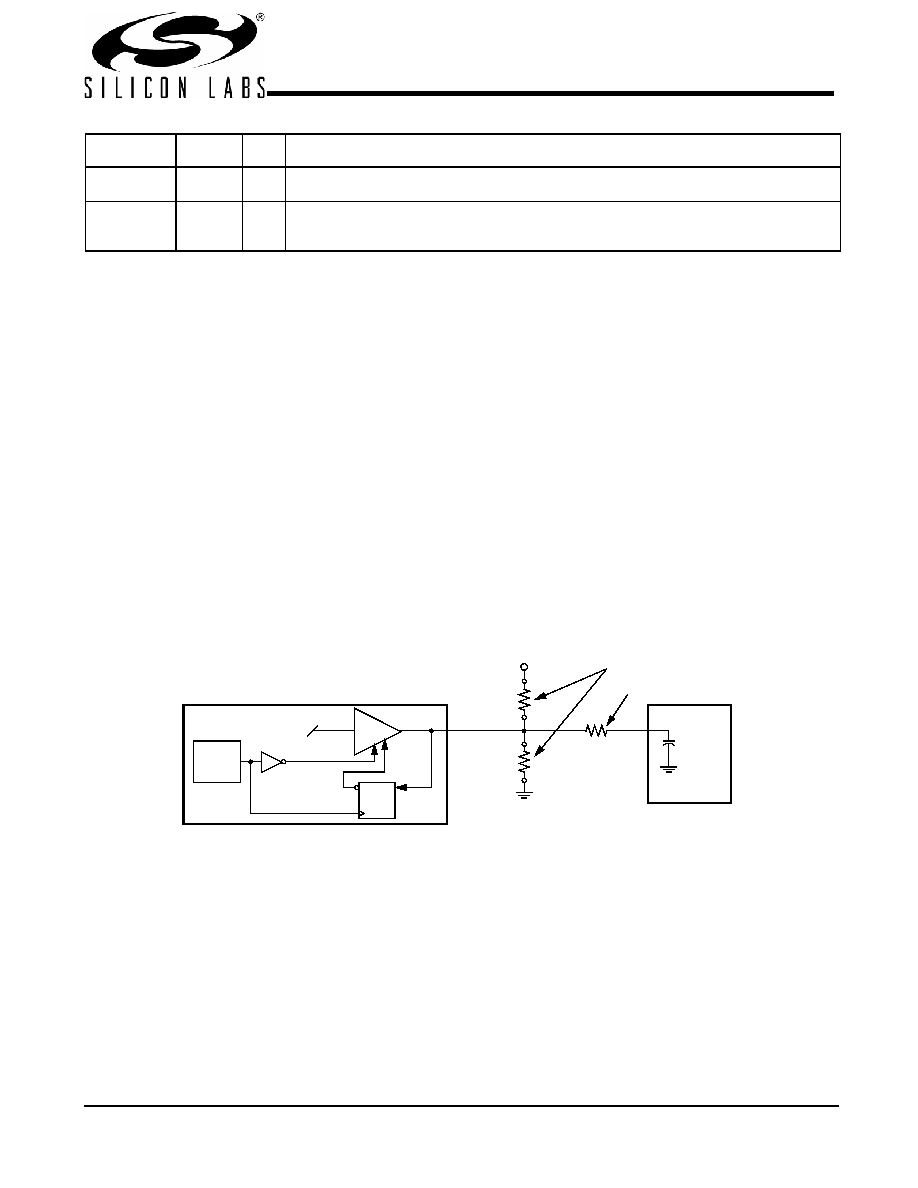
I/O Pin Operation
Pins 2, 8, 9, 29, and 30 are dual-purpose l/O pins. Upon
power-up these pins act as logic inputs, allowing the determi-
nation of assigned device functions. A short time after
power-up, the logic state of each pin is latched and the pins
become clock outputs. This feature reduces device pin count
by combining clock outputs with input select pins.
An external 10-k
“strapping” resistor is connected between
the l/O pin and ground or VDD. Connection to ground sets a
Figure 2 show two suggested methods for strapping resistor
connections.
Upon CYW150 power-up, the first 2 ms of operation are used
for input logic selection. During this period, the five I/O pins (2,
8, 9, 29, 30) are three-stated, allowing the output strapping
resistor on the l/O pins to pull the pins and their associated
capacitive clock load to either a logic HIGH or LOW state. At
the end of the 2-ms period, the established logic “0” or “1”
condition of the l/O pin is latched. Next the output buffer is
enabled, converting the l/O pins into operating clock outputs.
The 2-ms timer starts when VDD reaches 2.0V. The input bits
can only be reset by turning VDD off and then back on again.
It should be noted that the strapping resistors have no signif-
icant effect on clock output signal integrity. The drive
impedance of clock output (< 40
, nominal) is minimally
affected by the 10-k
strap to ground or V
DD. As with the
series termination resistor, the output strapping resistor should
be placed as close to the l/O pin as possible in order to keep
the interconnecting trace short. The trace from the resistor to
ground or VDD should be kept less than two inches in length
to minimize system noise coupling during input logic sampling.
When the clock outputs are enabled following the 2-ms input
period, the corresponding specified output frequency is
delivered on the pins, assuming that VDD has stabilized. If VDD
has not yet reached full value, output frequency initially may
be below target but will increase to target once VDD voltage
has stabilized. In either case, a short output clock cycle may
be produced from the CPU clock outputs when the outputs are
enabled.
VDDQ2
50, 56
P
Power Connection: Power supply for IOAPIC and CPU output buffers. Connect to 2.5V or
3.3V.
GND
4, 10, 23,
26, 34,
42, 48, 53
G
Ground Connections: Connect all ground pins to the common system ground plane.
Pin Definitions (continued)
Pin Name
Pin No.
Pin
Type
Pin Description
Power-on
Reset
Timer
Output Three-state
Data
Latch
Hold
QD
CYW150
VDD
Clock Load
10 k
Output
Buffer
(Load Option 1)
10 k
(Load Option 0)
Output
Low
Output Strapping Resistor
Series Termination Resistor
Figure 1. Input Logic Selection Through Resistor Load Option
相关PDF资料 |
PDF描述 |
|---|---|
| CYW173SXC | IC CLK GEN TAPE DRV 4CH 16SOIC |
| CYW305OXC | IC CLOCK W305 SOLANO 56SSOP |
| DAC5674IPHPG4 | IC DAC 14BIT 400MSPS 48-HTQFP |
| DAC7621EBG4 | IC SNGL 12BIT PARALLEL D/A 20SSO |
| DAC7801KPG4 | IC DUAL 12BIT CMOS DAC 24-DIP |
相关代理商/技术参数 |
参数描述 |
|---|---|
| CYW150OXCT | 功能描述:时钟发生器及支持产品 Legacy-440BX AGP Refer to W150 DS RoHS:否 制造商:Silicon Labs 类型:Clock Generators 最大输入频率:14.318 MHz 最大输出频率:166 MHz 输出端数量:16 占空比 - 最大:55 % 工作电源电压:3.3 V 工作电源电流:1 mA 最大工作温度:+ 85 C 安装风格:SMD/SMT 封装 / 箱体:QFN-56 |
| CYW152-12G | 制造商:Rochester Electronics LLC 功能描述:- Bulk |
| CYW15G0101DXB | 制造商:CYPRESS 制造商全称:Cypress Semiconductor 功能描述:Single-channel HOTLink II⑩ Transceiver |
| CYW15G0101DXB-BBC | 功能描述:电信线路管理 IC Sngl Ch XCVR COM RoHS:否 制造商:STMicroelectronics 产品:PHY 接口类型:UART 电源电压-最大:18 V 电源电压-最小:8 V 电源电流:30 mA 最大工作温度:+ 85 C 最小工作温度:- 40 C 安装风格:SMD/SMT 封装 / 箱体:VFQFPN-48 封装:Tray |
| CYW15G0101DXB-BBI | 功能描述:电信线路管理 IC Sngl Ch XCVR IND RoHS:否 制造商:STMicroelectronics 产品:PHY 接口类型:UART 电源电压-最大:18 V 电源电压-最小:8 V 电源电流:30 mA 最大工作温度:+ 85 C 最小工作温度:- 40 C 安装风格:SMD/SMT 封装 / 箱体:VFQFPN-48 封装:Tray |
发布紧急采购,3分钟左右您将得到回复。