- 您现在的位置:买卖IC网 > PDF目录373038 > DAC1208D650HN (NXP Semiconductors N.V.) Dual 12-bit DAC; up to 650 Msps; 2×, 4× or 8× interpolating PDF资料下载
参数资料
| 型号: | DAC1208D650HN |
| 厂商: | NXP Semiconductors N.V. |
| 元件分类: | 外设及接口 |
| 英文描述: | Dual 12-bit DAC; up to 650 Msps; 2×, 4× or 8× interpolating |
| 封装: | DAC1208D650HN/C1<SOT804-3|<<<1<Always Pb-free,;DAC1208D650HN/C1<SOT804-3|<<<1<Always Pb-free,; |
| 文件页数: | 12/98页 |
| 文件大小: | 557K |
| 代理商: | DAC1208D650HN |
第1页第2页第3页第4页第5页第6页第7页第8页第9页第10页第11页当前第12页第13页第14页第15页第16页第17页第18页第19页第20页第21页第22页第23页第24页第25页第26页第27页第28页第29页第30页第31页第32页第33页第34页第35页第36页第37页第38页第39页第40页第41页第42页第43页第44页第45页第46页第47页第48页第49页第50页第51页第52页第53页第54页第55页第56页第57页第58页第59页第60页第61页第62页第63页第64页第65页第66页第67页第68页第69页第70页第71页第72页第73页第74页第75页第76页第77页第78页第79页第80页第81页第82页第83页第84页第85页第86页第87页第88页第89页第90页第91页第92页第93页第94页第95页第96页第97页第98页
DAC1208D650
All information provided in this document is subject to legal disclaimers.
NXP B.V. 2010. All rights reserved.
Product data sheet
Rev. 2 — 14 December 2010
12 of 98
NXP Semiconductors
DAC1208D650
2
×
, 4
×
or 8
×
interpolating DAC with JESD204A interface
This device is MCDA-ML compliant, offering inter-lane alignment between several
devices. Samples alignment between devices is maintained up to output level because of
an NXP proprietary mechanism. One device is configured as the master and all the others
are configured as slaves. These will automatically align their output samples to the master
ones. Therefore, a system with several DAC1208D650s can produce data with a
guaranteed alignment of less than 1 DAC output clock period.
Each DAC generates two complementary current outputs on pins IOUTAP/IOUTAN and
IOUTBP/IOUTBN. This provides a full-scale output current of up to 20 mA. An internal
reference is available for the reference current which is externally adjustable using pin
VIRES.
The DAC1208D650 must be configured before operating. Therefore, it features an SPI
slave interface to access internal registers. Some of these registers also provide
information about the JESD204A interface status.
The DAC1208D650 requires supplies of both 3.3 V and 1.8 V. The 1.8 V supply has
separate digital and analog power supply pins. The clock input is LVDS compliant.
10.2 JESD204A receiver
The JEDEC204A defines the following parameters:
L is the number of lanes per link
M is the number of converters per device
F is the number of bytes per frame clock period
The DAC1208D650 supports both LMF = 421 and LMF = 211. The current setting is
configurable via the SPI registers interface.
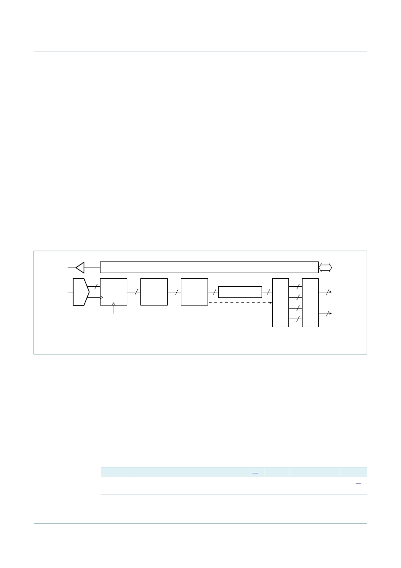
The complete Digital Layer Processing (DLP) adds a variable delay on each lane path.
This is mainly because of the inter-lane alignment.
Table 6.
Symbol Parameter
t
d
delay time
[1]
D = guaranteed by design.
[2]
Frame clock cycle.
The descrambler can be enabled/disabled
Fig 3.
JESD204A receiver
10b
10b
005aaa158
SYNC_OUT
internal
configuration
interface
DES
CLOCK
ALIGN
frame
clock
lane#
10b
12b
12b
SYNC
AND
WORD
ALIGN
8b
K-DETECT
10b/8b
8b
8b
8b
8b
8b
DESCRAMBLER
RX CONTROLLER
I
(
F
(
Digital Layer Processing Latency
Conditions
digital layer processing
delay
Test
[1]
D
Min
13
Typ
-
Max
28
Unit
cycle
[2]
相关PDF资料 |
PDF描述 |
|---|---|
| DAC1208D750HN | Dual 12-bit DAC; up to 750 Msps; 2×, 4× or 8× interpolating |
| DAC1208D750HN | Dual 12-bit DAC; up to 750 Msps; 2×, 4× or 8× interpolating |
| DL-5538S-C550-SB | 1270 nm ~ 1610 nm DFB LD MODULES 2.5 Gbps CWDM MQW-DFB LD RECEPTACLE |
| DL-5538S-C450-FB | 1270 nm ~ 1610 nm DFB LD MODULES 2.5 Gbps CWDM MQW-DFB LD RECEPTACLE |
| DL-5538S-C450-S | 1270 nm ~ 1610 nm DFB LD MODULES 2.5 Gbps CWDM MQW-DFB LD RECEPTACLE |
相关代理商/技术参数 |
参数描述 |
|---|---|
| DAC1208D650HN/C1,5 | 功能描述:数模转换器- DAC DL 12BIT DAC 650MSPS 2X 4X OR 8X INT RoHS:否 制造商:Texas Instruments 转换器数量:1 DAC 输出端数量:1 转换速率:2 MSPs 分辨率:16 bit 接口类型:QSPI, SPI, Serial (3-Wire, Microwire) 稳定时间:1 us 最大工作温度:+ 85 C 安装风格:SMD/SMT 封装 / 箱体:SOIC-14 封装:Tube |
| DAC1208D650HN-C1 | 制造商:Integrated Device Technology Inc 功能描述:HVQFN64 - Bulk |
| DAC1208D650HN-C18 | 制造商:Integrated Device Technology Inc 功能描述:HVQFN64 - Tape and Reel |
| DAC1208D650W1/DB,598 | 功能描述:数据转换 IC 开发工具 DAC DEMOBOARD RoHS:否 制造商:Texas Instruments 产品:Demonstration Kits 类型:ADC 工具用于评估:ADS130E08 接口类型:SPI 工作电源电压:- 6 V to + 6 V |
发布紧急采购,3分钟左右您将得到回复。