- 您现在的位置:买卖IC网 > PDF目录170654 > DAC1221E (TEXAS INSTRUMENTS INC) SERIAL INPUT LOADING, 1800 us SETTLING TIME, 16-BIT DAC, PDSO16 PDF资料下载
参数资料
| 型号: | DAC1221E |
| 厂商: | TEXAS INSTRUMENTS INC |
| 元件分类: | DAC |
| 英文描述: | SERIAL INPUT LOADING, 1800 us SETTLING TIME, 16-BIT DAC, PDSO16 |
| 封装: | SSOP-16 |
| 文件页数: | 14/16页 |
| 文件大小: | 154K |
| 代理商: | DAC1221E |
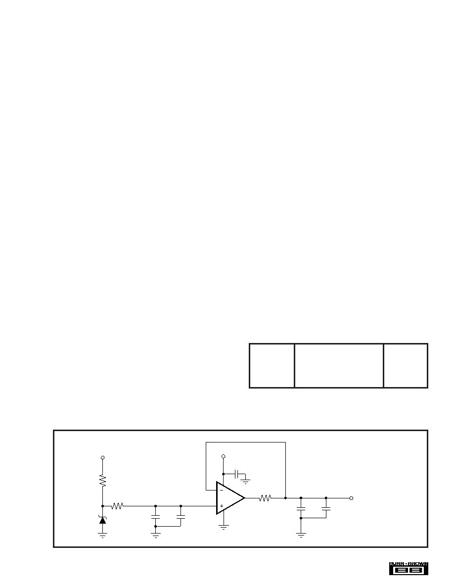
7
DAC1221
+
OPA336
2
7
3
1
6
4
+3V
87.6k
REF1004-1.2
20k
0.10
F
10
F
0.1
F
+
10
F
0.10
F
To V
REF Pin
100
FIGURE 2. Recommended External Voltage Reference Circuit for Best Low Noise Operation with the DAC1221.
Self Calibration
A self-calibration is performed after the bits “01” have been
written to the Command Register Operation Mode bits
(MD1 and MD0). This initiates a self-calibration on the next
clock cycle. The offset correction code is determined by a
repeated sequence of auto-zeroing the calibration compara-
tor to the offset reference and then comparing the DAC
output to the offset reference value. The end result is the
averaged, Offset Two’s Complement adjusted, and placed in
the OCR. The gain correction is done in a similar fashion,
except the correction is done against VREF to eliminate
common-mode errors. The FCR result represents the gain
code and is not Offset Two’s Complement adjusted.
The calibration function takes between 300ms and 500ms
(for fXIN = 2.5MHz) to complete. Once calibration is initi-
ated, further writing of register bits is disabled until calibra-
tion completes. The status of calibration can be verified by
reading the status of the Command Register Operation Mode
bits (MD1 and MD0). These bits will return to normal mode
“00” when calibration is complete.
It is recommended that the output be connected during
calibration. The output isolation is controlled by the CALPIN
bit in the CMR register. Setting the CALPIN bit will connect
the output and clearing the bit will disconnect and isolate the
output. Although it is recommended to connect the output
during calibration, the load impedance should be such that
the DAC1221 is not required to sink any current, but is able
to source up to the specified maximum.
Output Mode
The output of the DAC1221 can be synchronously reset.
By setting the CLR bit in the CMR, the data input register
is cleared to zero. This will result in an output of 0V when
DF = 1, or VREF when DF = 0.
The settling time is determined by the DISF and ADPT bits
of the command register. The default state of DISF = 0 and
ADPT = 0 enables fast settling, unless the output step is
small (
≈ 40mV). However, the DAC1221 can be forced to
always use fast settling if the ADPT bit is set to 1. If DISF
is set to 1, all fast settling is disabled.
The CRST bit of the CMR can be used to reset the offset and
calibration registers. By setting the CRST bit, the contents of
the calibration registers are reset to 0.
REFERENCE INPUT
The reference input voltage of 1.25V can be directly con-
nected to VREF pin.
The recommended reference circuit for the DAC1221 is
shown in Figure 2.
DIGITAL OPERATION
SYSTEM CONFIGURATION
The DAC1221 is controlled by 8-bit instruction codes (INSR)
and 16-bit command codes (CMR) via the serial interface,
which is externally clocked.
The DAC1221 Microcontroller (MC) consists of an ALU
and a register bank. The MC has three states: power-on
reset, calibration, and normal operation. In the power-on
reset state, the MC resets all the registers to their default
states. In the calibration state, the MC performs offset and
gain self-calibration. In the normal state, the MC performs
D/A conversions.
The DAC1221 has five internal registers, as shown in Table I.
Two of these, the Instruction Register (INSR) and the
Command Register (CMR), control the operation of the
converter. The Instruction Register utilizes an 8-bit instruc-
tion code to control the serial interface to determine whether
the next operation is either a read or a write, to control the
word length, and to select the appropriate register to
read/write. Communication with the DAC1221 is controlled
via the INSR. Under normal operation, the INSR is written
as the first part of each serial communication. The instruc-
tion that is sent determines what type of communication will
occur next. It is not possible to read the INSR. The Com-
mand Register has a 16-bit command code to set up the
INSR
Instruction Register
8 Bits
DIR
Data Input Register
16 Bits
CMR
Command Register
16 Bits
OCR
Offset Calibration Register
24 Bits
FCR
Full-Scale Calibration Register
24 Bits
TABLE I. DAC1221 Registers.
相关PDF资料 |
PDF描述 |
|---|---|
| DAC1221EG4 | SERIAL INPUT LOADING, 1800 us SETTLING TIME, 16-BIT DAC, PDSO16 |
| DAC5311IDCKR | SERIAL INPUT LOADING, 12 us SETTLING TIME, 8-BIT DAC, PDSO6 |
| DAC5311IDCKRG4 | SERIAL INPUT LOADING, 12 us SETTLING TIME, 8-BIT DAC, PDSO6 |
| DAC5311IDCKTG4 | SERIAL INPUT LOADING, 12 us SETTLING TIME, 8-BIT DAC, PDSO6 |
| DAC5652AIPFBRG4 | DUAL, PARALLEL, WORD INPUT LOADING, 0.02 us SETTLING TIME, 10-BIT DAC, PQFP48 |
相关代理商/技术参数 |
参数描述 |
|---|---|
| DAC1221E/2K5 | 制造商:Rochester Electronics LLC 功能描述:D/A CONV, 16-BIT 3V - Bulk |
| DAC1221EG4 | 功能描述:数模转换器- DAC 16B Delta-Sigma Low Power DAC RoHS:否 制造商:Texas Instruments 转换器数量:1 DAC 输出端数量:1 转换速率:2 MSPs 分辨率:16 bit 接口类型:QSPI, SPI, Serial (3-Wire, Microwire) 稳定时间:1 us 最大工作温度:+ 85 C 安装风格:SMD/SMT 封装 / 箱体:SOIC-14 封装:Tube |
| DAC1221LCN | 制造商:n/a 功能描述:1221 |
| DAC1221LCN/A+ | 制造商:未知厂家 制造商全称:未知厂家 功能描述:12-Bit Digital-to-Analog Converter |
| DAC1221LCN/B+ | 制造商:未知厂家 制造商全称:未知厂家 功能描述:12-Bit Digital-to-Analog Converter |
发布紧急采购,3分钟左右您将得到回复。