- 您现在的位置:买卖IC网 > PDF目录170654 > DAC1221E (TEXAS INSTRUMENTS INC) SERIAL INPUT LOADING, 1800 us SETTLING TIME, 16-BIT DAC, PDSO16 PDF资料下载
参数资料
| 型号: | DAC1221E |
| 厂商: | TEXAS INSTRUMENTS INC |
| 元件分类: | DAC |
| 英文描述: | SERIAL INPUT LOADING, 1800 us SETTLING TIME, 16-BIT DAC, PDSO16 |
| 封装: | SSOP-16 |
| 文件页数: | 2/16页 |
| 文件大小: | 154K |
| 代理商: | DAC1221E |
10
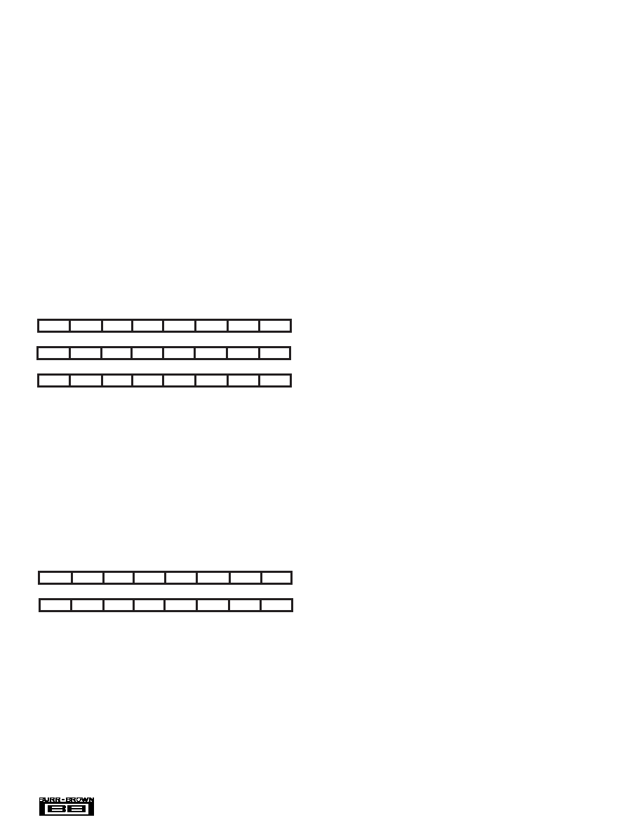
DAC1221
MSB
Byte 2
FCR23
FCR22
FCR21
FCR20
FCR19
FCR18
FCR17
FCR16
Byte 1
FCR15
FCR14
FCR13
FCR12
FCR11
FCR10
FCR9
FCR8
Byte 0
LSB
FCR7
FCR6
FCR5
FCR4
FCR3
FCR2
FCR1
FCR0
TABLE VI. Full-Scale Calibration Register.
MSB
Byte 1
DIR15
DIR14
DIR13
DIR12
DIR11
DIR10
DIR9
DIR8
Byte 0
LSB
DIR7
DIR6
DIR5
DIR4
DIR3
DIR2
DIR1
DIR0
TABLE VII. Data Input Register.
Full-Scale Calibration Register (FCR)
The FCR is a 24-bit register which contains the full-scale
correction factor that is applied to the digital input before it
is transferred to the modulator. The contents of this register
will be the result of a self-calibration, or written to by the
user.
The FCR is both readable and writable via the serial inter-
face. For applications requiring a more accurate calibration,
a calibration can be performed, the results averaged, and a
more precise value written back to the FCR.
The actual FCR value will change from part to part and with
configuration, temperature, and power supply.
In addition, be aware that the contents of the FCR are not
used to directly correct the digital input. Rather, the correc-
tion is a function of the FCR value. This function is linear
and two known points can be used as a basis of interpolating
intermediate values for the FCR. The contents of the FCR
are in unsigned binary format. This is not affected by the DF
bit in the Command Register.
Data Input Register (DIR)
The DIR is a 16-bit register which contains the digital input
value (see Table VII). The register is latched on the falling
edge of the last bit of the last byte sent. The contents of the
DIR are then loaded into the modulator. This means that the
DIR register can be updated after sending 1 or 2 bytes, which
is determined by the MB1 and MB0 bits in the Instruction
Register. The contents of the DIR can be Offset Two’s
Complement or Straight Binary.
SLEEP MODE
The Sleep Mode is entered after the bit combination 10 has
been written to the CMR Operation Mode bits (MD1 and
MD0). This mode ends when these bits are changed to a
value other than 10.
Communication with the DAC1221 can continue during
Sleep Mode. When a new mode (other than Sleep) has been
entered, the DAC1221 will execute a very brief internal
power-up sequence of the analog and digital circuitry. In
addition, the settling of the external VREF and other circuitry
must be taken into account to determine the amount of time
required to resume normal operation.
Once serial communication is resumed, the Sleep Mode is
exited by changing the MD1 - MD0 bits to any other mode.
When a new mode (other than Sleep) has been entered, the
DAC1221 will execute a very brief internal power-up se-
quence of the analog and digital circuitry. In addition, the
settling of the external VREF and other circuitry must be
taken into account to determine the amount of time required
to resume normal operation.
SERIAL INTERFACE
The DAC1221 includes a flexible serial interface which can
be connected to microcontrollers and digital signal proces-
sors in a variety of ways. Along with this flexibility, there is
also a good deal of complexity. This section describes the
trade-offs between the different types of interfacing methods
in a top-down approach—starting with the overall flow and
control of serial data, moving to specific interface examples,
and then providing information on various issues related to
the serial interface.
Reset, Power-On Reset and Brown-Out
The DAC1221 contains an internal power-on reset circuit. If
the power supply ramp rate is greater than 50mV/ms, this
circuit will be adequate to ensure the device powers up
correctly. Due to oscillator settling considerations, commu-
nication to and from the DAC1221 should not occur for at
least 25ms after power is stable.
If this requirement cannot be met or if the circuit has brown-
out considerations, the timing diagram of Figure 3 can be
used to reset the DAC1221. This accomplishes the reset by
controlling the duty cycle of the SCLK input.
Sleep mode is the default state after power on or reset. The
output is high impedance during sleep mode.
相关PDF资料 |
PDF描述 |
|---|---|
| DAC1221EG4 | SERIAL INPUT LOADING, 1800 us SETTLING TIME, 16-BIT DAC, PDSO16 |
| DAC5311IDCKR | SERIAL INPUT LOADING, 12 us SETTLING TIME, 8-BIT DAC, PDSO6 |
| DAC5311IDCKRG4 | SERIAL INPUT LOADING, 12 us SETTLING TIME, 8-BIT DAC, PDSO6 |
| DAC5311IDCKTG4 | SERIAL INPUT LOADING, 12 us SETTLING TIME, 8-BIT DAC, PDSO6 |
| DAC5652AIPFBRG4 | DUAL, PARALLEL, WORD INPUT LOADING, 0.02 us SETTLING TIME, 10-BIT DAC, PQFP48 |
相关代理商/技术参数 |
参数描述 |
|---|---|
| DAC1221E/2K5 | 制造商:Rochester Electronics LLC 功能描述:D/A CONV, 16-BIT 3V - Bulk |
| DAC1221EG4 | 功能描述:数模转换器- DAC 16B Delta-Sigma Low Power DAC RoHS:否 制造商:Texas Instruments 转换器数量:1 DAC 输出端数量:1 转换速率:2 MSPs 分辨率:16 bit 接口类型:QSPI, SPI, Serial (3-Wire, Microwire) 稳定时间:1 us 最大工作温度:+ 85 C 安装风格:SMD/SMT 封装 / 箱体:SOIC-14 封装:Tube |
| DAC1221LCN | 制造商:n/a 功能描述:1221 |
| DAC1221LCN/A+ | 制造商:未知厂家 制造商全称:未知厂家 功能描述:12-Bit Digital-to-Analog Converter |
| DAC1221LCN/B+ | 制造商:未知厂家 制造商全称:未知厂家 功能描述:12-Bit Digital-to-Analog Converter |
发布紧急采购,3分钟左右您将得到回复。