- 您现在的位置:买卖IC网 > PDF目录170654 > DAC5672AIPFBR (TEXAS INSTRUMENTS INC) DUAL, PARALLEL, WORD INPUT LOADING, 0.02 us SETTLING TIME, 14-BIT DAC, PQFP48 PDF资料下载
参数资料
| 型号: | DAC5672AIPFBR |
| 厂商: | TEXAS INSTRUMENTS INC |
| 元件分类: | DAC |
| 英文描述: | DUAL, PARALLEL, WORD INPUT LOADING, 0.02 us SETTLING TIME, 14-BIT DAC, PQFP48 |
| 封装: | GREEN, PLASTIC, TQFP-48 |
| 文件页数: | 5/26页 |
| 文件大小: | 1097K |
| 代理商: | DAC5672AIPFBR |
GSET
MODE
Internal
DigitalIn
DVDD
400W
100kW
DGND
Input Interfaces
Dual-Bus Data Interface and Timing
www.ti.com................................................................................................................................................... SLAS528A – SEPTEMBER 2007 – REVISED MAY 2009
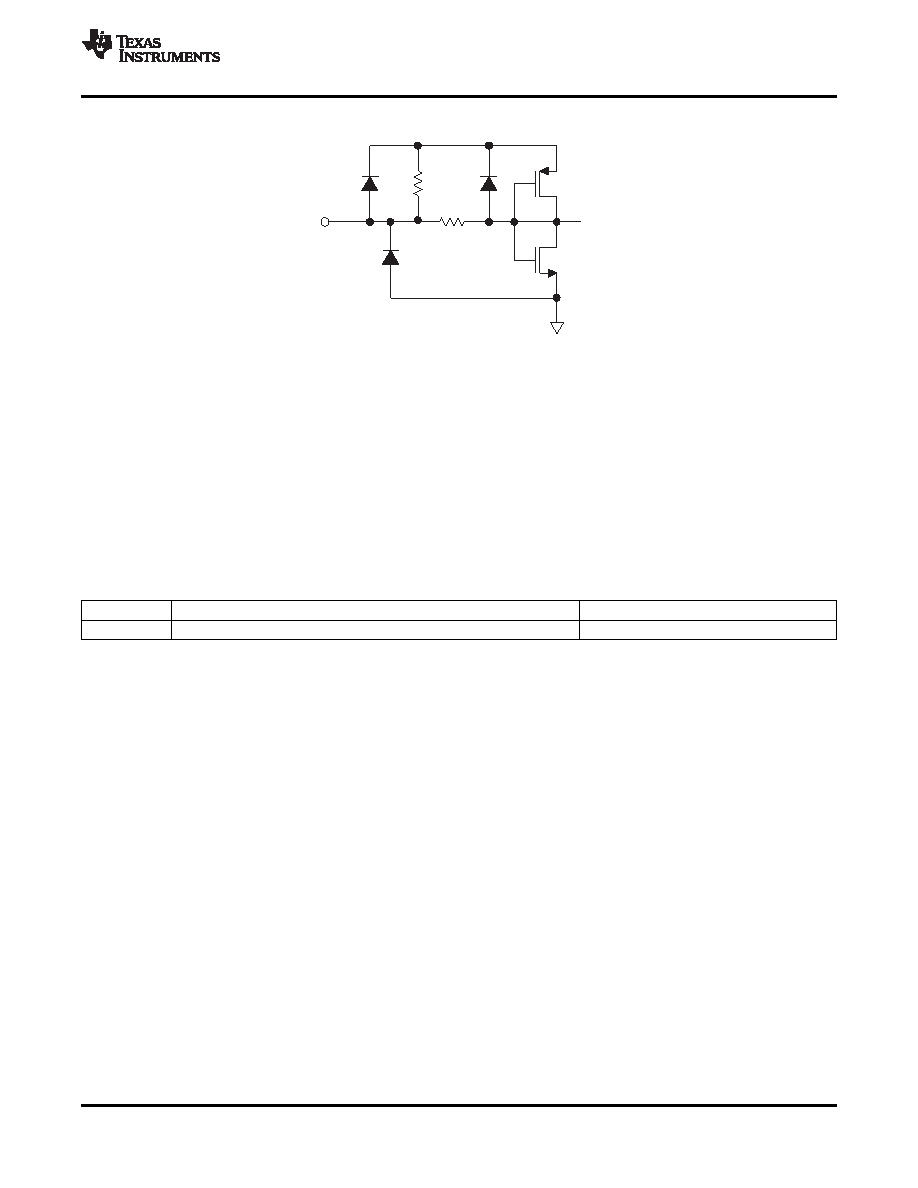
Figure 18. CMOS/TTL Digital Equivalent Input With Internal Pullup Resistor
The DAC5672A features two operating modes selected by the MODE pin, as shown in Table 1.
For dual-bus input mode, the device essentially consists of two separate DACs. Each DAC has its own
separate data input bus, clock input, and data write signal (data latch-in).
In single-bus interleaved mode, the data must be presented interleaved at the A-channel input bus. The
B-channel input bus is not used in this mode. The clock and write input are now shared by both DACs.
Table 1. Operating Modes
MODE Pin
MODE pin connected to DGND
MODE pin connected to DVDD
Bus input
Single-bus interleaved mode, clock and write input equal for both DACs
Dual-bus mode, DACs operate independently
In dual-bus mode, the MODE pin is connected to DVDD. The two converter channels within the DAC5672A
consist of two independent, 14-bit, parallel data ports. Each DAC channel is controlled by its own set of write
(WRTA, WRTB) and clock (CLKA, CLKB) lines. The WRTA/B lines control the channel input latches and the
CLKA/B lines control the DAC latches. The data is first loaded into the input latch by a rising edge of the
WRTA/B line.
The internal data transfer requires a correct sequence of write and clock inputs, since essentially two clock
domains having equal periods (but possibly different phases) are input to the DAC5672A. This is defined by a
minimum requirement of the time between the rising edge of the clock and the rising edge of the write inputs.
This essentially implies that the rising edge of CLKA/B must occur at the same time or before the rising edge of
the WRTA/B signal. A minimum delay of 2 ns must be maintained if the rising edge of the clock occurs after the
rising edge of the write. Note that these conditions are satisfied when the clock and write inputs are connected
externally. Note that all specifications were measured with the WRTA/B and CLKA/B lines connected together.
Copyright 2007–2009, Texas Instruments Incorporated
13
Product Folder Link(s): DAC5672A
相关PDF资料 |
PDF描述 |
|---|---|
| DAC5687IPZP | PARALLEL, WORD INPUT LOADING, 0.0104 us SETTLING TIME, 16-BIT DAC, PQFP100 |
| DAC5687IPZPG4 | PARALLEL, WORD INPUT LOADING, 0.0104 us SETTLING TIME, 16-BIT DAC, PQFP100 |
| DAC5688IRGCTG4 | PARALLEL, WORD INPUT LOADING, 0.0104 us SETTLING TIME, 16-BIT DAC, PQCC64 |
| DAC702LH | PARALLEL, WORD INPUT LOADING, 4 us SETTLING TIME, 16-BIT DAC, CDIP24 |
| DAC7545KUG4 | PARALLEL, WORD INPUT LOADING, 2 us SETTLING TIME, 12-BIT DAC, PDSO20 |
相关代理商/技术参数 |
参数描述 |
|---|---|
| DAC5672AIPFBRG4 | 功能描述:数模转换器- DAC 14B 275MSPS Dual DAC RoHS:否 制造商:Texas Instruments 转换器数量:1 DAC 输出端数量:1 转换速率:2 MSPs 分辨率:16 bit 接口类型:QSPI, SPI, Serial (3-Wire, Microwire) 稳定时间:1 us 最大工作温度:+ 85 C 安装风格:SMD/SMT 封装 / 箱体:SOIC-14 封装:Tube |
| DAC5672-EP | 制造商:TI 制造商全称:Texas Instruments 功能描述:DUAL 14-BIT 200-MSPS DIGITAL-TO-ANALOG CONVERTER |
| DAC5672EVM | 功能描述:数据转换 IC 开发工具 DAC5672 Eval Mod RoHS:否 制造商:Texas Instruments 产品:Demonstration Kits 类型:ADC 工具用于评估:ADS130E08 接口类型:SPI 工作电源电压:- 6 V to + 6 V |
| DAC5672IPFB | 功能描述:数模转换器- DAC Digital to Analog Converter RoHS:否 制造商:Texas Instruments 转换器数量:1 DAC 输出端数量:1 转换速率:2 MSPs 分辨率:16 bit 接口类型:QSPI, SPI, Serial (3-Wire, Microwire) 稳定时间:1 us 最大工作温度:+ 85 C 安装风格:SMD/SMT 封装 / 箱体:SOIC-14 封装:Tube |
| DAC5672IPFB | 制造商:Texas Instruments 功能描述:IC DAC 14BIT 275MSPS 制造商:Texas Instruments 功能描述:IC, DAC, 14BIT, 275MSPS, TQFP-48 |
发布紧急采购,3分钟左右您将得到回复。