- 您现在的位置:买卖IC网 > PDF目录170654 > DAC7545JP (TEXAS INSTRUMENTS INC) PARALLEL, WORD INPUT LOADING, 2 us SETTLING TIME, 12-BIT DAC, PDIP20 PDF资料下载
参数资料
| 型号: | DAC7545JP |
| 厂商: | TEXAS INSTRUMENTS INC |
| 元件分类: | DAC |
| 英文描述: | PARALLEL, WORD INPUT LOADING, 2 us SETTLING TIME, 12-BIT DAC, PDIP20 |
| 封装: | PLASTIC, MS-001AD, DIP-20 |
| 文件页数: | 7/14页 |
| 文件大小: | 552K |
| 代理商: | DAC7545JP |
DAC7545
2
SBAS150A
www.ti.com
ABSOLUTE MAXIMUM RATINGS(1)
T
A = +25°C, unless otherwise noted.
VDD to DGND ........................................................................... –0.3V, +17
Digital Input to DGND ............................................................... –0.3V, VDD
VRFB, VREF, to DGND ........................................................................ ±25V
VPIN 1 to DGND ........................................................................ –0.3V, VDD
AGND to DGND ........................................................................ –0.3V, VDD
Power Dissipation: Any Package to +75
°C .................................... 450mW
Derates above +75
°C by ................................ 6mW/°C
Operating Temperature:
Commercial J, K, L, and GL ........................................... –40
°C to +85°C
Storage Temperature ...................................................... –65
°C to +150°C
Lead Temperature (soldering, 10s) ............................................... +300
°C
NOTE: (1) Stresses above those listed above may cause permanent damage to
the device. This is a stress rating only and functional operation of the device at
these or any other condition above those indicated in the operational sections of
this specification is not implied. Exposure to absolute maximum rating conditions
for extended periods may affect device reliability.
ELECTROSTATIC
DISCHARGE SENSITIVITY
This integrated circuit can be damaged by ESD. Texas Instru-
ments recommends that all integrated circuits be handled with
appropriate precautions. Failure to observe proper handling
and installation procedures can cause damage.
ESD damage can range from subtle performance degrada-
tion to complete device failure. Precision integrated circuits
may be more susceptible to damage because very small
parametric changes could cause the device not to meet its
published specifications.
SPECIFIED
RELATIVE
GAIN ERROR (LSB)
PACKAGE
TEMPERATURE
PACKAGE
ORDERING
TRANSPORT
PRODUCT
ACCURACY (LSB)
VDD = +5V
PACKAGE-LEAD DESIGNATOR(1)
RANGE
MARKING
NUMBER
MEDIA, QUANTITY
DAC7545
±2
±20
SO-20
DW
–40
°C to +85°C DAC7545JU
DAC7545JU
Rails, 38
"
±1
±10
"
DAC7545KU
Rails, 38
DAC7545
±1/2
±5
SO-20
DW
–40
°C to +85°C DAC7545LU
DAC7545LU
Rails, 38
"
±1/2
±2
"
DAC7545GLU DAC7545GLU
Rails, 38
NOTE: (1) For the most current specifications and package information, refer to our web site at www.ti.com.
PACKAGE/ORDERING INFORMATION
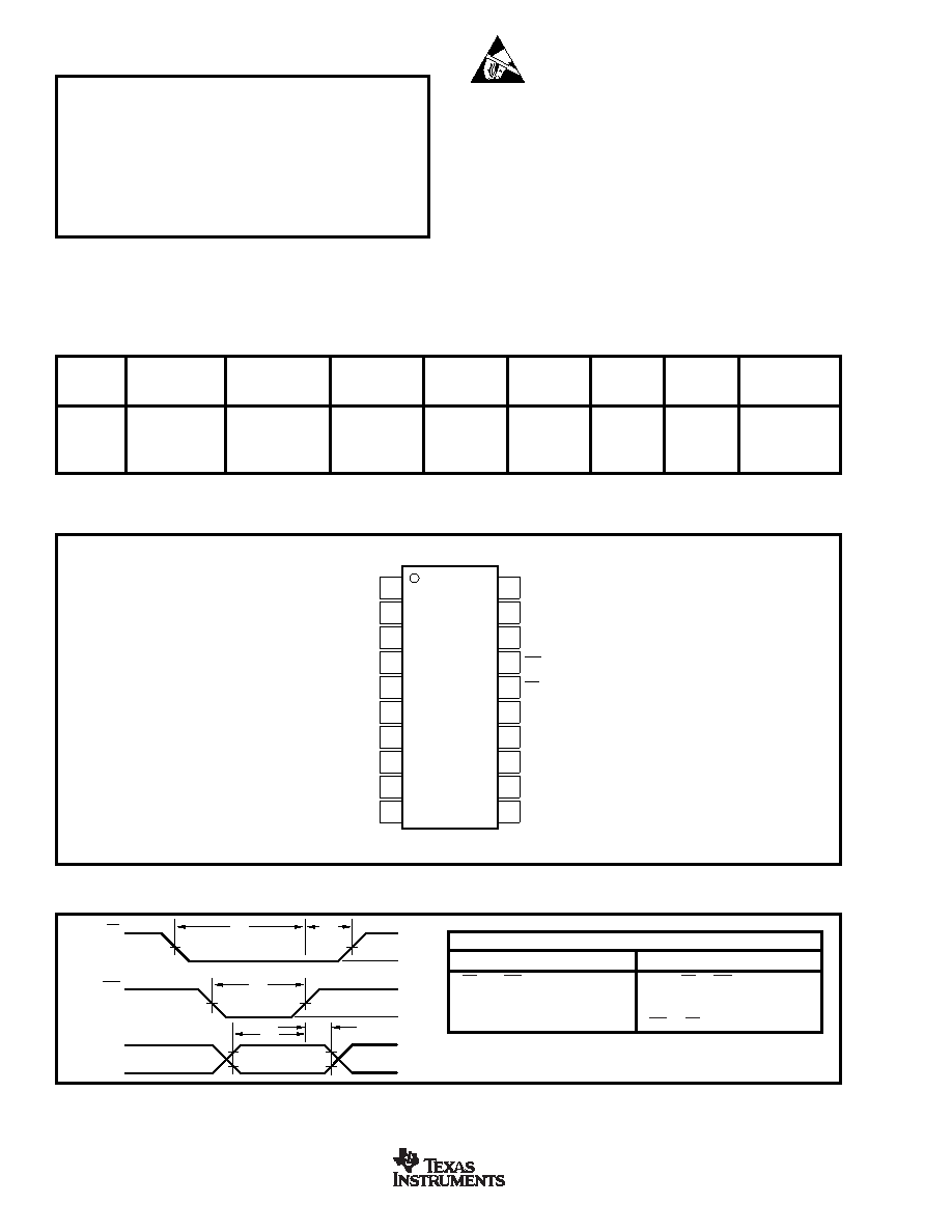
PIN CONNECTIONS
DAC7545
1
2
3
4
5
6
7
8
9
10
20
19
18
17
16
15
14
13
12
11
OUT 1
AGND
DGND
(MSB) DB
11
DB
10
DB
9
DB
8
DB
7
DB
6
DB
5
R
FB
V
REF
V
DD
WR
CS
DB
0 (LSB)
DB
1
DB
2
DB
3
DB
4
Top View
SO
WRITE CYCLE TIMING DIAGRAM
Mode Selection
Write Mode
Hold Mode
CS and WR low, DAC responds
Either CS or WR high, data bus to
Data Bus (DB0-DB11) inputs.
(DB0-DB11) is locked out; DAC
holds last data present when
WR or CS assumed high state.
NOTES: VDD = +5V, tR = tF = 20ns. VDD = +15V, tR = tF = 40ns. All inputs signal
rise and fall times measured from 10% to 90% of VDD. Timing measurement
reference level is (VIH + VIL)/2.
t
DS
t
DH
V
IH
V
IL
Data
Valid
V
DD
0
t
WR
t
CS
t
CH
V
DD
0
V
DD
0
Data In
(DB
0-DB11)
WR
CS
相关PDF资料 |
PDF描述 |
|---|---|
| DAC7545KP | PARALLEL, WORD INPUT LOADING, 2 us SETTLING TIME, 12-BIT DAC, PDIP20 |
| DAC7554IDGSR | SERIAL INPUT LOADING, 5 us SETTLING TIME, 12-BIT DAC, PDSO10 |
| DAC7554IDGS | SERIAL INPUT LOADING, 5 us SETTLING TIME, 12-BIT DAC, PDSO10 |
| DAC7612U | SERIAL INPUT LOADING, 7 us SETTLING TIME, 12-BIT DAC, PDSO8 |
| DAC7612UBG4 | SERIAL INPUT LOADING, 7 us SETTLING TIME, 12-BIT DAC, PDSO8 |
相关代理商/技术参数 |
参数描述 |
|---|---|
| DAC7545JU | 功能描述:数模转换器- DAC CMOS 12-Bit Multiplying RoHS:否 制造商:Texas Instruments 转换器数量:1 DAC 输出端数量:1 转换速率:2 MSPs 分辨率:16 bit 接口类型:QSPI, SPI, Serial (3-Wire, Microwire) 稳定时间:1 us 最大工作温度:+ 85 C 安装风格:SMD/SMT 封装 / 箱体:SOIC-14 封装:Tube |
| DAC7545JUG4 | 功能描述:数模转换器- DAC CMOS 12-Bit Multiplying RoHS:否 制造商:Texas Instruments 转换器数量:1 DAC 输出端数量:1 转换速率:2 MSPs 分辨率:16 bit 接口类型:QSPI, SPI, Serial (3-Wire, Microwire) 稳定时间:1 us 最大工作温度:+ 85 C 安装风格:SMD/SMT 封装 / 箱体:SOIC-14 封装:Tube |
| DAC7545KP | 制造商:Texas Instruments 功能描述:DAC SGL R-2R 12-BIT 24SSOP - Rail/Tube |
| DAC7545KU | 功能描述:数模转换器- DAC CMOS 12-Bit Multiplying RoHS:否 制造商:Texas Instruments 转换器数量:1 DAC 输出端数量:1 转换速率:2 MSPs 分辨率:16 bit 接口类型:QSPI, SPI, Serial (3-Wire, Microwire) 稳定时间:1 us 最大工作温度:+ 85 C 安装风格:SMD/SMT 封装 / 箱体:SOIC-14 封装:Tube |
| DAC7545KU-1 | 制造商:Rochester Electronics LLC 功能描述:- Bulk |
发布紧急采购,3分钟左右您将得到回复。