- 您现在的位置:买卖IC网 > PDF目录170654 > DAC7625U/1KG4 (TEXAS INSTRUMENTS INC) PARALLEL, WORD INPUT LOADING, 5 us SETTLING TIME, 12-BIT DAC, PDSO28 PDF资料下载
参数资料
| 型号: | DAC7625U/1KG4 |
| 厂商: | TEXAS INSTRUMENTS INC |
| 元件分类: | DAC |
| 英文描述: | PARALLEL, WORD INPUT LOADING, 5 us SETTLING TIME, 12-BIT DAC, PDSO28 |
| 封装: | GREEN, SOIC-28 |
| 文件页数: | 6/19页 |
| 文件大小: | 473K |
| 代理商: | DAC7625U/1KG4 |
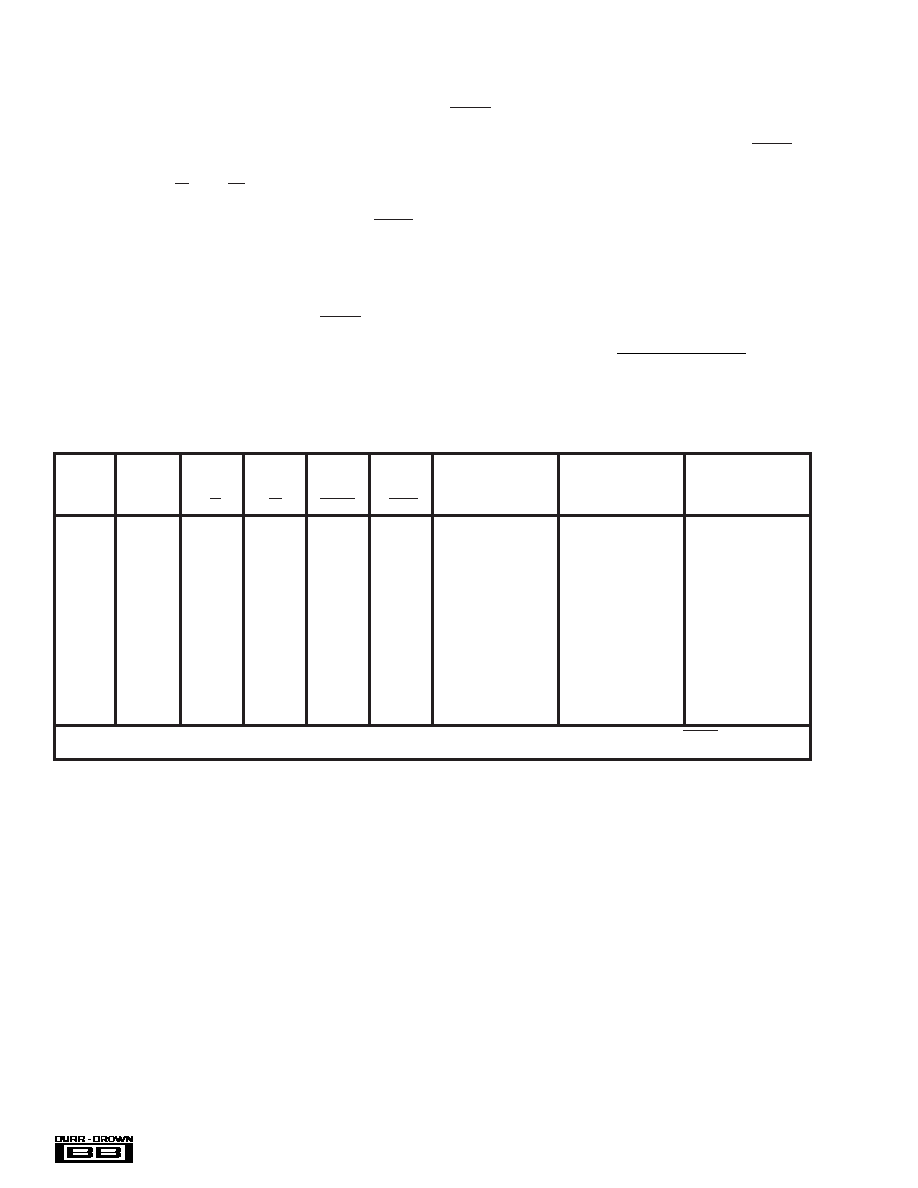
14
DAC7724, 7725
V
OUT = V REFL +
V
REFH –V REFL
()N
4096
STATE OF
SELECTED
STATE OF
INPUT
ALL DAC
A1
A0
R/W
CS
RESET
LDAC
REGISTER
REGISTERS
L(1)
LLL
H(2)
L
A
Transparent
L
H
L
H
L
B
Transparent
H
L
H
L
C
Transparent
H
L
H
L
D
Transparent
LLLL
H
A
Transparent
Latched
L
H
L
H
B
Transparent
Latched
H
L
H
C
Transparent
Latched
H
L
H
D
Transparent
Latched
L
H
L
H
A
Readback
Latched
L
H
L
H
B
Readback
Latched
H
L
H
L
H
C
Readback
Latched
H
L
H
D
Readback
Latched
X(3)
X
H
L
NONE
(All Latched)
Transparent
X
H
NONE
(All Latched)
Latched
XXXX
L
X
ALL
Reset(4)
NOTES: (1) L = Logic LOW. (2) H= Logic HIGH. (3) X = Don’t Care. (4) DAC7724 resets to 800H, DAC7725 resets to 000H. When RESET rises, all registers
that are in their latched state retain the reset value.
TABLE I. DAC7724 and DAC7725 Control Logic Truth Table.
DIGITAL INTERFACE
Table I shows the basic control logic for the DAC7724/25.
Note that each internal register is level triggered and not
edge triggered. When the appropriate signal is LOW, the
register becomes transparent. When this signal is returned
HIGH, the digital word currently in the register is latched.
The first set of registers (the Input Registers) are triggered
via the A0, A1, R/W, and CS inputs. Only one of these
registers is transparent at any given time. The second set of
registers (the DAC Registers) are all transparent when LDAC
input is pulled LOW.
Each DAC can be updated independently by writing to the
appropriate Input Register and then updating the DAC
Register. Alternatively, the entire DAC Register set can be
configured as always transparent by keeping LDAC LOW—
the DAC update will occur when the Input Register is
written.
The double buffered architecture is mainly designed so that
each DAC Input Register can be written at any time and then
all DAC output voltages updated simultaneously by pulling
LDAC LOW. It also allows a DAC Input Register to be
written to at any point and the DAC voltage to be synchro-
nously changed via a trigger signal connected to LDAC.
DIGITAL TIMING
Figure 4 and Table II provide detailed timing for the digital
interface of the DAC7724 and DAC7725.
DIGITAL INPUT CODING
The DAC7724 and DAC7725 input data is in straight binary
format. The output voltage is given by the following equa-
tion:
where N is the digital input code. This equation does not
include the effects of offset (zero-scale) errors.
相关PDF资料 |
PDF描述 |
|---|---|
| DAC7643VFBTG4 | PARALLEL, WORD INPUT LOADING, 8 us SETTLING TIME, 16-BIT DAC, PQFP32 |
| DAC7654YTG4 | SERIAL INPUT LOADING, 12 us SETTLING TIME, 16-BIT DAC, PQFP64 |
| DAC7714U | QUAD, SERIAL INPUT LOADING, 8 us SETTLING TIME, 12-BIT DAC, PDSO16 |
| DAC7801LUG4 | PARALLEL, 8 BITS INPUT LOADING, 0.4 us SETTLING TIME, 12-BIT DAC, PDSO24 |
| DAC7800LU | SERIAL INPUT LOADING, 0.4 us SETTLING TIME, 12-BIT DAC, PDSO16 |
相关代理商/技术参数 |
参数描述 |
|---|---|
| DAC7625UB | 功能描述:数模转换器- DAC 12-Bit Quad Voltage Output RoHS:否 制造商:Texas Instruments 转换器数量:1 DAC 输出端数量:1 转换速率:2 MSPs 分辨率:16 bit 接口类型:QSPI, SPI, Serial (3-Wire, Microwire) 稳定时间:1 us 最大工作温度:+ 85 C 安装风格:SMD/SMT 封装 / 箱体:SOIC-14 封装:Tube |
| DAC7625UB | 制造商:Texas Instruments 功能描述:Digital/Analog Converter IC Interface Ty |
| DAC7625UB/1K | 功能描述:数模转换器- DAC 12-Bit Quad Voltage Output RoHS:否 制造商:Texas Instruments 转换器数量:1 DAC 输出端数量:1 转换速率:2 MSPs 分辨率:16 bit 接口类型:QSPI, SPI, Serial (3-Wire, Microwire) 稳定时间:1 us 最大工作温度:+ 85 C 安装风格:SMD/SMT 封装 / 箱体:SOIC-14 封装:Tube |
| DAC7625UB/1KG4 | 功能描述:数模转换器- DAC 12-Bit Quad Voltage Output RoHS:否 制造商:Texas Instruments 转换器数量:1 DAC 输出端数量:1 转换速率:2 MSPs 分辨率:16 bit 接口类型:QSPI, SPI, Serial (3-Wire, Microwire) 稳定时间:1 us 最大工作温度:+ 85 C 安装风格:SMD/SMT 封装 / 箱体:SOIC-14 封装:Tube |
| DAC7625UBG4 | 功能描述:数模转换器- DAC 12-Bit Quad Voltage Output RoHS:否 制造商:Texas Instruments 转换器数量:1 DAC 输出端数量:1 转换速率:2 MSPs 分辨率:16 bit 接口类型:QSPI, SPI, Serial (3-Wire, Microwire) 稳定时间:1 us 最大工作温度:+ 85 C 安装风格:SMD/SMT 封装 / 箱体:SOIC-14 封装:Tube |
发布紧急采购,3分钟左右您将得到回复。