参数资料
| 型号: | DAC8043GPZ |
| 厂商: | Analog Devices Inc |
| 文件页数: | 3/16页 |
| 文件大小: | 0K |
| 描述: | IC DAC 12BIT MULTIPLY CMOS 8-DIP |
| 产品培训模块: | Data Converter Fundamentals DAC Architectures |
| 标准包装: | 1 |
| 设置时间: | 250ns |
| 位数: | 12 |
| 数据接口: | 串行 |
| 转换器数目: | 1 |
| 电压电源: | 单电源 |
| 功率耗散(最大): | 500µW |
| 工作温度: | -40°C ~ 85°C |
| 安装类型: | 通孔 |
| 封装/外壳: | 8-DIP(0.300",7.62mm) |
| 供应商设备封装: | 8-PDIP |
| 包装: | 管件 |
| 输出数目和类型: | 1 电流,单极;1 电流,双极 |
| 采样率(每秒): | 366k |
DAC8043
Rev. E | Page 11 of 16
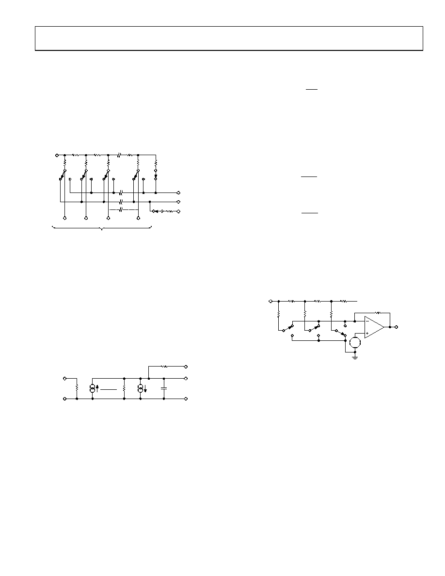
To further ensure accuracy across the full temperature range,
permanently on MOS switches were included in series with
the feedback resistor and the terminating resistor of the R-2R
ladder. The simplified DAC circuit, Figure 13, shows the location
of the series switches. These series switches are equivalently
scaled to two times Switch S1 (MSB) and to Switch S12 (LSB),
respectively, to maintain constant relative voltage drops with
varying temperature. During any testing of the resistor ladder
or RFEEDBACK (such as incoming inspection), VDD must be present
to turn on these series switches.
00271-
013
20k
20k
20k
GND
IOUT
RFEEDBACK
S12
S3
20k
S2
20k
S1
VREF
10k
10k
*THESE SWITCHES PERMANENTLY ON.
10k
10k
BIT 1 (MSB)
BIT 2
DIGITAL INPUTS
(SWITCHES SHOWN FOR DIGITAL INPUTS (HIGH))
BIT 3
BIT 12 (LSB)
*
Figure 13. Simplified DAC Circuit
EQUIVALENT CIRCUIT ANALYSIS
Figure 14 shows an equivalent analog circuit for the DAC8043.
The (D × VREF)/R current source is code dependent and is the
current generated by the DAC. The current source, ILKG, consists
of surface and junction leakages and doubles approximately
every 10°C. COUT is the output capacitance; it is the result of
the N-channel MOS switches and varies from 80 pF to 110 pF,
depending on the digital input code. RO is the equivalent out-
put resistance that also varies with digital input code. R is the
nominal R-2R resistor ladder resistance.
00271-
014
R
COUT
RFB
IOUT
VREF
GND
ILKG
D × VREF
R
Figure 14. Equivalent Analog Circuit
DYNAMIC PERFORMANCE
Output Impedance
The output resistance of the DAC8043, as in the case of the
output capacitance, varies with the digital input code. This
resistance, looking back into the IOUT terminal, may be between
10 k (the feedback resistor alone when all digital inputs are low)
and 7.5 k (the feedback resistor in parallel with approximately
30 k of the R-2R ladder network resistance when any single bit
logic is high). Static accuracy and dynamic performance will be
affected by these variations. This variation is best illustrated by
using the circuit of Figure 15 and the following equation:
+
=
O
FB
OS
ERROR
R
V
1
where:
RO is a function of the digital code and
= 10 k for more than four bits of Logic 1.
= 30 k for any single bit of Logic 1.
Therefore, the offset gain varies as follows:
At Code 0011 1111 1111,
OS
1
ERROR
V
2
kΩ
10
kΩ
10
1
=
+
=
At Code 0100 0000 0000,
OS
2
ERROR
V
3
/
4
kΩ
30
kΩ
10
1
=
+
=
The error difference is 2/3 VOS.
Because one LSB has a weight (for VREF = 10 V) of 2.4 mV for
the DAC8043, it is clearly important that VOS be minimized,
either by using the amplifier’s nulling pins or an external nulling
network or by selecting an amplifier with inherently low VOS.
and OP42.
00271-
015
RFB
VREF
2R
ETC
R
OP77
VOS
Figure 15. Simplified Circuit
The gain and phase stability of the output amplifier, board
layout, and power supply decoupling all affect the dynamic
performance. The use of a small compensation capacitor may
be required when high speed operational amplifiers are used. It
may be connected across the feedback resistor of the amplifier
to provide the necessary phase compensation to critically damp
the output. The output capacitance of the DAC8043 and the RFB
resistor form a pole that must be outside the amplifier’s unity
gain crossover frequency.
The considerations when using high speed amplifiers are:
1. Phase compensation (see Figure 16 and Figure 17).
2. Power supply decoupling at the device socket and the use
of proper grounding techniques.
相关PDF资料 |
PDF描述 |
|---|---|
| AD7528LNZ | IC DAC 8BIT DUAL MULTIPLY 20-DIP |
| AD7225LR | IC DAC 8BIT QUAD W/AMP 24-SOIC |
| AD5570ARSZ-REEL | IC DAC 16BIT SERIAL IN 16SSOP |
| VI-2TK-IV-F4 | CONVERTER MOD DC/DC 40V 150W |
| VI-2TJ-IV-F3 | CONVERTER MOD DC/DC 36V 150W |
相关代理商/技术参数 |
参数描述 |
|---|---|
| DAC8043HP | 制造商:Analog Devices 功能描述: 制造商:PMI/AD 功能描述: |
| DAC8043U | 功能描述:数模转换器- DAC 12bit Multiply D/A RoHS:否 制造商:Texas Instruments 转换器数量:1 DAC 输出端数量:1 转换速率:2 MSPs 分辨率:16 bit 接口类型:QSPI, SPI, Serial (3-Wire, Microwire) 稳定时间:1 us 最大工作温度:+ 85 C 安装风格:SMD/SMT 封装 / 箱体:SOIC-14 封装:Tube |
| DAC8043U | 制造商:Texas Instruments 功能描述:D/A Converter (D-A) IC 制造商:Texas Instruments 功能描述:IC, DAC, 12BIT, 284KSPS, SOIC-8 |
| DAC8043U/2K5 | 功能描述:数模转换器- DAC 12bit Multiply D/A RoHS:否 制造商:Texas Instruments 转换器数量:1 DAC 输出端数量:1 转换速率:2 MSPs 分辨率:16 bit 接口类型:QSPI, SPI, Serial (3-Wire, Microwire) 稳定时间:1 us 最大工作温度:+ 85 C 安装风格:SMD/SMT 封装 / 箱体:SOIC-14 封装:Tube |
| DAC8043U/2K5G4 | 功能描述:数模转换器- DAC 12bit Multiply D/A RoHS:否 制造商:Texas Instruments 转换器数量:1 DAC 输出端数量:1 转换速率:2 MSPs 分辨率:16 bit 接口类型:QSPI, SPI, Serial (3-Wire, Microwire) 稳定时间:1 us 最大工作温度:+ 85 C 安装风格:SMD/SMT 封装 / 箱体:SOIC-14 封装:Tube |
发布紧急采购,3分钟左右您将得到回复。