参数资料
| 型号: | DAC8222GPZ |
| 厂商: | Analog Devices Inc |
| 文件页数: | 4/15页 |
| 文件大小: | 0K |
| 描述: | IC DAC 12BIT DUAL W/BUFF 24DIP |
| 产品培训模块: | Data Converter Fundamentals DAC Architectures |
| 标准包装: | 15 |
| 设置时间: | 1µs |
| 位数: | 12 |
| 转换器数目: | 2 |
| 电压电源: | 单电源 |
| 工作温度: | 0°C ~ 70°C |
| 安装类型: | 通孔 |
| 封装/外壳: | 24-DIP(0.300",7.62mm) |
| 供应商设备封装: | 24-PDIP |
| 包装: | 管件 |
| 输出数目和类型: | 2 电流,单极;2 电流,双极 |
| 采样率(每秒): | 1M |
DAC8222
–12–
REV. C
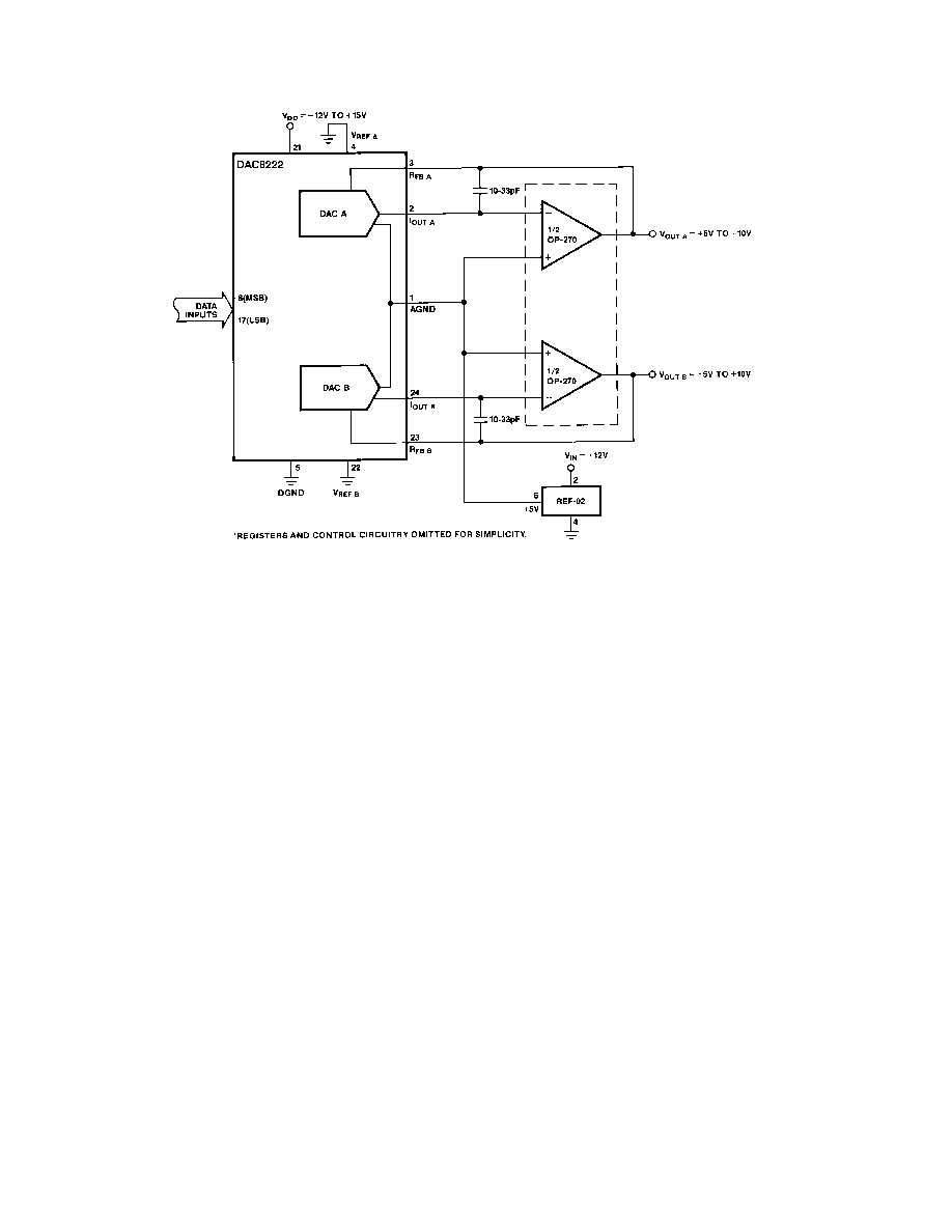
Figure 26. Single Supply Operation (Current Switching Mode)
SINGLE SUPPLY OPERATION
CURRENT STEERING MODE
Because the DAC8222’s R-2R resistor ladder terminating resis-
tor is internally connected to AGND, it lends itself well to single
supply operation in the current steering mode. This means that
AGND can be raised above system ground as shown in Figure 26.
The output voltage range will be from +5 V to +10 V depending
on the digital input code and is given by:
VOUT = VOS + (n/4096) (VOS)
where VOS = Offset Reference Voltage (+5 V in Figure 26)
where n = Decimal Equivalent of the Digital Input Word
VOLTAGE SWITCHING MODE
Figure 27 shows the DAC8222 in a single supply voltage
switching mode of operation. In this configuration, the DAC’s
R-2R ladder acts as a voltage divider. The output voltage at the
VREF pin exhibits a constant impedance R (typically 11 k
) and
must be buffered by an op amp. RFB pins are not used in this
circuit configuration. The reference input voltage must be main-
tained within +1.25 V of AGND and VDD from +12 V to +15 V
to preserve device accuracy.
The output voltage expression is given by:
VOUT = VREF (n/4096)
where n = Decimal Equivalent of the Digital Input Word
APPLICATIONS TIPS
GENERAL GROUND MANAGEMENT
Grounding techniques should be tailored to each individual sys-
tem. Ground loops should be avoided, and ground current
paths should be as short as possible and have a low impedance.
The DAC8222’s AGND and DGND pins should be tied to-
gether at the device socket to prevent digital transients from ap-
pearing at the analog output. This common point then becomes
the single ground point connection. AGND and DGND should
then be brought out separately and tied to their respective power
supply grounds. Ground loops can be created if both grounds
are tied together at more than one location, i.e., tied together at
the device and at the digital and analog power supplies.
A PC board ground plane can be used for the single point
ground connection should the connections not be practical at
the device socket. If neither of these connections is practical or
allowed, the device should be placed as close as possible to the
system’s single point ground connection. Back-to-back Schottky
diodes should then be connected between AGND and DGND.
POWER SUPPLY DECOUPLING
Power supplies used with the DAC8222 should be well filtered
and regulated. Local supply decoupling consisting of a 1
F to
10
F tantalum capacitor in parallel with a 0.1 F ceramic is
highly recommended. The capacitors should be connected be-
tween the VDD and DGND pins and at the device socket.
相关PDF资料 |
PDF描述 |
|---|---|
| DAC8229FSZ-REEL | IC DAC 8BIT DUAL V-OUT 20SOIC |
| DAC8248FS | IC DAC 12BIT DUAL W/BUFF 24-SOIC |
| DAC8408GP | IC DAC 8BIT QUAD W/MEMORY 28-DIP |
| DAC8413EP | IC DAC 12BIT QUAD V-OUT 28-DIP |
| DAC8420FQ | IC DAC 12BIT QUAD SRL LP 16-CDIP |
相关代理商/技术参数 |
参数描述 |
|---|---|
| DAC8222HP | 制造商:Rochester Electronics LLC 功能描述:- Bulk |
| DAC8222HS | 制造商:Rochester Electronics LLC 功能描述:- Bulk |
| DAC8228 | 制造商:AD 制造商全称:Analog Devices 功能描述:Dual 8-Bit CMOS D/A Converter with Voltage Output |
| DAC8228FP | 功能描述:IC DAC 8BIT DUAL V-OUT 20-DIP RoHS:否 类别:集成电路 (IC) >> 数据采集 - 数模转换器 系列:- 标准包装:2,400 系列:- 设置时间:- 位数:18 数据接口:串行 转换器数目:3 电压电源:模拟和数字 功率耗散(最大):- 工作温度:-40°C ~ 85°C 安装类型:表面贴装 封装/外壳:36-TFBGA 供应商设备封装:36-TFBGA 包装:带卷 (TR) 输出数目和类型:* 采样率(每秒):* |
| DAC8228FPZ | 功能描述:IC DAC 8BIT DUAL V-OUT 20DIP RoHS:是 类别:集成电路 (IC) >> 数据采集 - 数模转换器 系列:- 标准包装:47 系列:- 设置时间:2µs 位数:14 数据接口:并联 转换器数目:1 电压电源:单电源 功率耗散(最大):55µW 工作温度:-40°C ~ 85°C 安装类型:表面贴装 封装/外壳:28-SSOP(0.209",5.30mm 宽) 供应商设备封装:28-SSOP 包装:管件 输出数目和类型:1 电流,单极;1 电流,双极 采样率(每秒):* |
发布紧急采购,3分钟左右您将得到回复。