参数资料
| 型号: | DAC8248FPZ |
| 厂商: | Analog Devices Inc |
| 文件页数: | 16/16页 |
| 文件大小: | 0K |
| 描述: | IC DAC 12BIT DUAL BUFFERD 24DIP |
| 产品培训模块: | Data Converter Fundamentals DAC Architectures |
| 标准包装: | 15 |
| 设置时间: | 1µs |
| 位数: | 12 |
| 数据接口: | 并联 |
| 转换器数目: | 2 |
| 电压电源: | 单电源 |
| 功率耗散(最大): | 50µW |
| 工作温度: | -40°C ~ 85°C |
| 安装类型: | 通孔 |
| 封装/外壳: | 24-DIP(0.300",7.62mm) |
| 供应商设备封装: | 24-PDIP |
| 包装: | 管件 |
| 输出数目和类型: | 2 电流,单极;2 电流,双极 |
| 采样率(每秒): | 1M |
DAC8248
–9–
REV. B
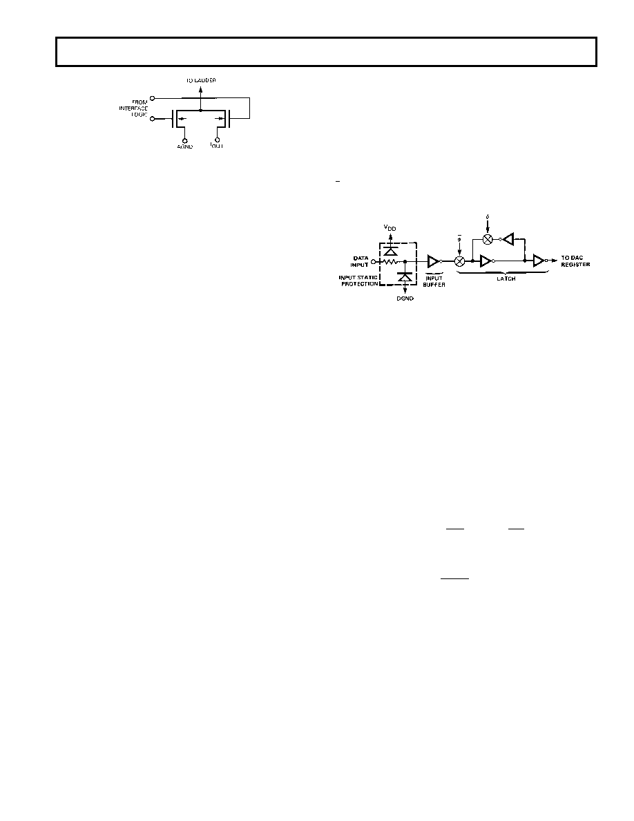
Figure 2. N-Channel Current Steering Switch
The binary-weighted currents are switched between IOUT and
AGND by the transistor switches. Selection between IOUT and
AGND is determined by the digital input code. It is important
to keep the voltage difference between IOUT and AGND termi-
nals as close to zero as practical to preserve data sheet limits. It
is easily accomplished by connecting the DAC’s AGND to the
noninverting input of an operational amplifier and IOUT to the
inverting input. The amplifier’s feedback resistor can be elimi-
nated by connecting the op amp’s output directly to the DAC’s
RFB terminal (by using the DAC’s internal feedback resistor,
RFB). The amplifier also provides the current-to-voltage conver-
sion for the DAC’s output current.
The output voltage is dependent on the DAC’s digital input
code and VREF, and is given by:
VOUT = VREF × D/4096
where D is the digital input code integer number that is between
0 and 4095.
The DAC’s input resistance, RREF, is always equal to a constant
value, R. This means that VREF can be driven by a reference
voltage or current, ac or dc (positive or negative). It is recom-
mended that a low temperature-coefficient external RFB resistor
be used if a current source is employed.
The DAC’s output capacitance (COUT) is code dependent and
varies from 90 pF (all digital inputs low) to 120 pF (all digital
inputs high).
To ensure accuracy over the full operating temperature range,
permanently turned “ON” MOS transistor switches were in-
cluded in series with the feedback resistor (RFB) and the R-2R
ladder’s terminating resistor (see Figure 1). The gates of these
NMOS transistors are internally connected to VDD and will be
turned “OFF” (open) if VDD is not applied. If an op amp is us-
ing the DAC’s RFB resistor to close its feedback loop, then VDD
must be applied before or at the same time as the op amp’s sup-
ply; this will prevent the op amp’s output from becoming “open
circuited” and swinging to either rail. In addition, some applica-
tions require the DAC’s ladder resistance to fall within a certain
range and are measured at incoming inspection; VDD must be
applied before these measurements can be made.
DIGITAL SECTION
The DAC8248’s digital inputs are TTL compatible at VDD = +5 V
and CMOS compatible at VDD = +15 V. They were designed to
convert TTL and CMOS input logic levels into voltage levels that
will drive the internal circuitry. The DAC8248 can use +5 V
CMOS logic levels with VDD = +12 V; however, supply current
will increase to approximately 5 mA–6 mA.
Figure 3 shows the DAC’s digital input structure for one bit.
This circuitry drives the DAC registers. Digital controls,
φ and
φ, shown are generated from the DAC’s input control logic
circuitry.
Figure 3. Digital Input Structure For One Bit
The digital inputs are electrostatic-discharge (ESD) protected
with two internal distributed diodes as shown in Figure 3; they
are connected between VDD and DGND. Each input has a typi-
cal input current of less than 1 nA.
The digital inputs are CMOS inverters and draw supply current
when operating in their linear region. Using a +5 V supply, the
linear region is between +1.2 V to +2.8 V with current peaking
at +1.8 V. Using a +15 V supply, the linear region is from
+1.2 V to +12 V (current peaking at +3.9 V). It is recom-
mended that the digital inputs be operated as close to the power
supply voltage and DGND as is practically possible; this will
keep supply currents to a minimum. The DAC8248 may be
operated with any supply voltage between the range of +5 V to
+15 V and still perform to data sheet limits.
The DAC8248’s 8-bit wide data port loads a 12-bit word in two
bytes: 8-bits then 4-bits (or 4-bits first then 8-bits, at users dis-
cretion) in a right justified data format. This data is loaded into
the input registers with the LSB/MSB and WR control pins.
Data transfer from the input registers to the DAC registers can
be automatic. It can occur upon loading of the second data byte
into the input register, or can occur at a later time through a
strobed transfer using the LDAC control pin.
相关PDF资料 |
PDF描述 |
|---|---|
| LTC1596BCSW#PBF | IC D/A CONV 16BIT MLTPLYNG16SOIC |
| AD7837BRZ | IC DAC 12BIT DUAL MULT 24-SOIC |
| AD660ARZ | IC DAC 16BIT MONO W/VREF 24-SOIC |
| ABFT-40.000MHZ-T | FREQ TRANSLATOR JITTER ATTEN |
| UTS6JC1210S | CONN PLUG CABLE 10X1.0 FEMALE |
相关代理商/技术参数 |
参数描述 |
|---|---|
| DAC8248FPZ | 制造商:Analog Devices 功能描述:12BIT DAC CMOS DUAL 8248 DIP24 |
| DAC8248FS | 功能描述:IC DAC 12BIT DUAL W/BUFF 24-SOIC RoHS:否 类别:集成电路 (IC) >> 数据采集 - 数模转换器 系列:- 产品培训模块:Lead (SnPb) Finish for COTS Obsolescence Mitigation Program 标准包装:1,000 系列:- 设置时间:1µs 位数:8 数据接口:串行 转换器数目:8 电压电源:双 ± 功率耗散(最大):941mW 工作温度:0°C ~ 70°C 安装类型:表面贴装 封装/外壳:24-SOIC(0.295",7.50mm 宽) 供应商设备封装:24-SOIC W 包装:带卷 (TR) 输出数目和类型:8 电压,单极 采样率(每秒):* |
| DAC8248FS-REEL | 功能描述:IC DAC 12BIT DUAL W/BUFF 24-SOIC RoHS:否 类别:集成电路 (IC) >> 数据采集 - 数模转换器 系列:- 产品培训模块:Data Converter Fundamentals DAC Architectures 标准包装:750 系列:- 设置时间:7µs 位数:16 数据接口:并联 转换器数目:1 电压电源:双 ± 功率耗散(最大):100mW 工作温度:0°C ~ 70°C 安装类型:表面贴装 封装/外壳:28-LCC(J 形引线) 供应商设备封装:28-PLCC(11.51x11.51) 包装:带卷 (TR) 输出数目和类型:1 电压,单极;1 电压,双极 采样率(每秒):143k |
| DAC8248FSZ | 功能描述:IC DAC 12BIT DUAL W/BUFF 24SOIC RoHS:是 类别:集成电路 (IC) >> 数据采集 - 数模转换器 系列:- 标准包装:1 系列:- 设置时间:4.5µs 位数:12 数据接口:串行,SPI? 转换器数目:1 电压电源:单电源 功率耗散(最大):- 工作温度:-40°C ~ 125°C 安装类型:表面贴装 封装/外壳:8-SOIC(0.154",3.90mm 宽) 供应商设备封装:8-SOICN 包装:剪切带 (CT) 输出数目和类型:1 电压,单极;1 电压,双极 采样率(每秒):* 其它名称:MCP4921T-E/SNCTMCP4921T-E/SNRCTMCP4921T-E/SNRCT-ND |
| DAC8248FSZ-REEL | 功能描述:IC DAC 12BIT DUAL W/BUFF 24SOIC RoHS:是 类别:集成电路 (IC) >> 数据采集 - 数模转换器 系列:- 产品培训模块:Data Converter Fundamentals DAC Architectures 标准包装:750 系列:- 设置时间:7µs 位数:16 数据接口:并联 转换器数目:1 电压电源:双 ± 功率耗散(最大):100mW 工作温度:0°C ~ 70°C 安装类型:表面贴装 封装/外壳:28-LCC(J 形引线) 供应商设备封装:28-PLCC(11.51x11.51) 包装:带卷 (TR) 输出数目和类型:1 电压,单极;1 电压,双极 采样率(每秒):143k |
发布紧急采购,3分钟左右您将得到回复。