参数资料
| 型号: | DAC8248FPZ |
| 厂商: | Analog Devices Inc |
| 文件页数: | 3/16页 |
| 文件大小: | 0K |
| 描述: | IC DAC 12BIT DUAL BUFFERD 24DIP |
| 产品培训模块: | Data Converter Fundamentals DAC Architectures |
| 标准包装: | 15 |
| 设置时间: | 1µs |
| 位数: | 12 |
| 数据接口: | 并联 |
| 转换器数目: | 2 |
| 电压电源: | 单电源 |
| 功率耗散(最大): | 50µW |
| 工作温度: | -40°C ~ 85°C |
| 安装类型: | 通孔 |
| 封装/外壳: | 24-DIP(0.300",7.62mm) |
| 供应商设备封装: | 24-PDIP |
| 包装: | 管件 |
| 输出数目和类型: | 2 电流,单极;2 电流,双极 |
| 采样率(每秒): | 1M |
DAC8248
–11–
REV. B
AUTOMATIC DATA TRANSFER MODE
Data may be transferred automatically from the input register to
the DAC register. The first cycle loads the first data byte into
the input register; the second cycle loads the second data byte
and simultaneously transfers the full 12-bit data word to the
DAC register. It takes four cycles to load and transfer two com-
plete digital words for both DAC’s, see Figure 4 (Four Cycle
Update Timing Diagram) and the Mode Selection Table.
STROBED DATA TRANSFER MODE
Strobed data transfer allows the full 12-bit digital word to be
loaded into the input registers and transferred to the DAC regis-
ters at a later time. This transfer mode requires five cycles: four
to load two new data words into both DACs, and the fifth to
transfer all data into the DAC registers. See Figure 5 (Five Cycle
Update Timing Diagram) and the Mode Selection Table.
Strobed data transfer separating data loading and transfer op-
erations serves two functions: the DAC output updating may be
more precisely controlled, and multiple DACs in a multiple
DAC system can be updated simultaneously.
RESET
The DAC8248 comes with a RESET pin that is useful in system
calibration cycles and/or during system power-up. All registers
are reset to zero when RESET is low, and latched at zero on the
rising edge of the RESET signal when WRITE is high.
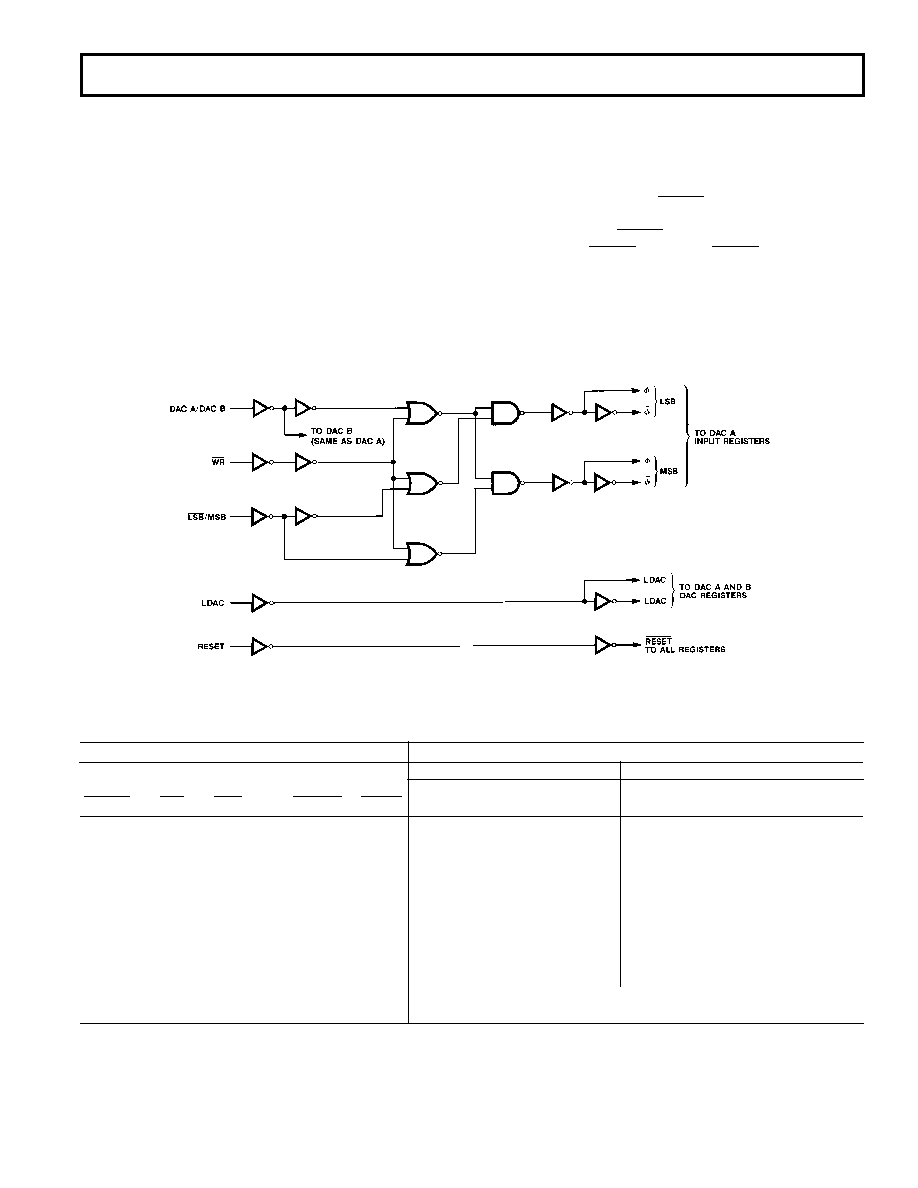
INTERFACE CONTROL LOGIC
The DAC8248’s control logic is shown in Figure 6. This cir-
cuitry interfaces with the system bus and controls the DAC
functions.
Figure 6. Input Control Logic
MODE SELECTION TABLE
DIGITAL INPUTS
REGISTER STATUS
DAC A
DAC B
Input Register
DAC
Input Register
DAC
DAC A
/B
WR
LSB
/MSB
RESET
LDAC
LSB
MSB
Register
LSB
MSB
Register
L
H
WR
LAT
L
H
L
WR
LAT
WR
LAT
WR
L
H
LAT
WR
LAT
L
H
L
LAT
WR
LAT
WR
H
L
H
LAT
WR
LAT
H
L
H
L
LAT
WR
LAT
WR
H
L
H
LAT
WR
LAT
H
L
H
L
LAT
WR
LAT
WR
X
H
X
H
LAT
X
H
X
H
L
LAT
WR
LAT
WR
X
L
X
ALL REGISTERS ARE RESET TO ZEROS
XH
X
g
X
ZEROS ARE LATCHED IN ALL REGISTERS
L = Low, H = High, X = Don’t Care, WR = Registers Being Loaded, LAT = Registers Latched.
相关PDF资料 |
PDF描述 |
|---|---|
| LTC1596BCSW#PBF | IC D/A CONV 16BIT MLTPLYNG16SOIC |
| AD7837BRZ | IC DAC 12BIT DUAL MULT 24-SOIC |
| AD660ARZ | IC DAC 16BIT MONO W/VREF 24-SOIC |
| ABFT-40.000MHZ-T | FREQ TRANSLATOR JITTER ATTEN |
| UTS6JC1210S | CONN PLUG CABLE 10X1.0 FEMALE |
相关代理商/技术参数 |
参数描述 |
|---|---|
| DAC8248FPZ | 制造商:Analog Devices 功能描述:12BIT DAC CMOS DUAL 8248 DIP24 |
| DAC8248FS | 功能描述:IC DAC 12BIT DUAL W/BUFF 24-SOIC RoHS:否 类别:集成电路 (IC) >> 数据采集 - 数模转换器 系列:- 产品培训模块:Lead (SnPb) Finish for COTS Obsolescence Mitigation Program 标准包装:1,000 系列:- 设置时间:1µs 位数:8 数据接口:串行 转换器数目:8 电压电源:双 ± 功率耗散(最大):941mW 工作温度:0°C ~ 70°C 安装类型:表面贴装 封装/外壳:24-SOIC(0.295",7.50mm 宽) 供应商设备封装:24-SOIC W 包装:带卷 (TR) 输出数目和类型:8 电压,单极 采样率(每秒):* |
| DAC8248FS-REEL | 功能描述:IC DAC 12BIT DUAL W/BUFF 24-SOIC RoHS:否 类别:集成电路 (IC) >> 数据采集 - 数模转换器 系列:- 产品培训模块:Data Converter Fundamentals DAC Architectures 标准包装:750 系列:- 设置时间:7µs 位数:16 数据接口:并联 转换器数目:1 电压电源:双 ± 功率耗散(最大):100mW 工作温度:0°C ~ 70°C 安装类型:表面贴装 封装/外壳:28-LCC(J 形引线) 供应商设备封装:28-PLCC(11.51x11.51) 包装:带卷 (TR) 输出数目和类型:1 电压,单极;1 电压,双极 采样率(每秒):143k |
| DAC8248FSZ | 功能描述:IC DAC 12BIT DUAL W/BUFF 24SOIC RoHS:是 类别:集成电路 (IC) >> 数据采集 - 数模转换器 系列:- 标准包装:1 系列:- 设置时间:4.5µs 位数:12 数据接口:串行,SPI? 转换器数目:1 电压电源:单电源 功率耗散(最大):- 工作温度:-40°C ~ 125°C 安装类型:表面贴装 封装/外壳:8-SOIC(0.154",3.90mm 宽) 供应商设备封装:8-SOICN 包装:剪切带 (CT) 输出数目和类型:1 电压,单极;1 电压,双极 采样率(每秒):* 其它名称:MCP4921T-E/SNCTMCP4921T-E/SNRCTMCP4921T-E/SNRCT-ND |
| DAC8248FSZ-REEL | 功能描述:IC DAC 12BIT DUAL W/BUFF 24SOIC RoHS:是 类别:集成电路 (IC) >> 数据采集 - 数模转换器 系列:- 产品培训模块:Data Converter Fundamentals DAC Architectures 标准包装:750 系列:- 设置时间:7µs 位数:16 数据接口:并联 转换器数目:1 电压电源:双 ± 功率耗散(最大):100mW 工作温度:0°C ~ 70°C 安装类型:表面贴装 封装/外壳:28-LCC(J 形引线) 供应商设备封装:28-PLCC(11.51x11.51) 包装:带卷 (TR) 输出数目和类型:1 电压,单极;1 电压,双极 采样率(每秒):143k |
发布紧急采购,3分钟左右您将得到回复。