- 您现在的位置:买卖IC网 > PDF目录170654 > DAC8413FPCZ-REEL (ANALOG DEVICES INC) QUAD, PARALLEL, WORD INPUT LOADING, 10 us SETTLING TIME, 12-BIT DAC, PQCC28 PDF资料下载
参数资料
| 型号: | DAC8413FPCZ-REEL |
| 厂商: | ANALOG DEVICES INC |
| 元件分类: | DAC |
| 英文描述: | QUAD, PARALLEL, WORD INPUT LOADING, 10 us SETTLING TIME, 12-BIT DAC, PQCC28 |
| 封装: | PLASTIC, MO-047AB, LCC-28 |
| 文件页数: | 6/20页 |
| 文件大小: | 531K |
| 代理商: | DAC8413FPCZ-REEL |
DAC8412/DAC8413
Rev. F | Page 14 of 20
THEORY OF OPERATION
INTRODUCTION
The DAC8412/DAC8413 are quad, voltage output, 12-bit parallel
input DACs featuring a 12-bit data bus with readback capability.
The only differences between the DAC8412/DAC8413 are the
reset functions. The DAC8412 resets to midscale (Code 0x800),
and the DAC8413 resets to minimum scale (Code 0x000).
The ability to operate from a single 5 V supply is a unique
feature of these DACs.
Operation of the DAC8412/DAC8413 can be viewed by
dividing the system into three separate functional groups: the
digital I/O and logic, the digital-to-analog converters, and the
output amplifiers.
DACS
Each DAC is a voltage switched, high impedance (R = 50 kΩ),
R-2R ladder configuration. Each 2R resistor is driven by a pair
of switches that connect the resistor to either VREFH or VREFL.
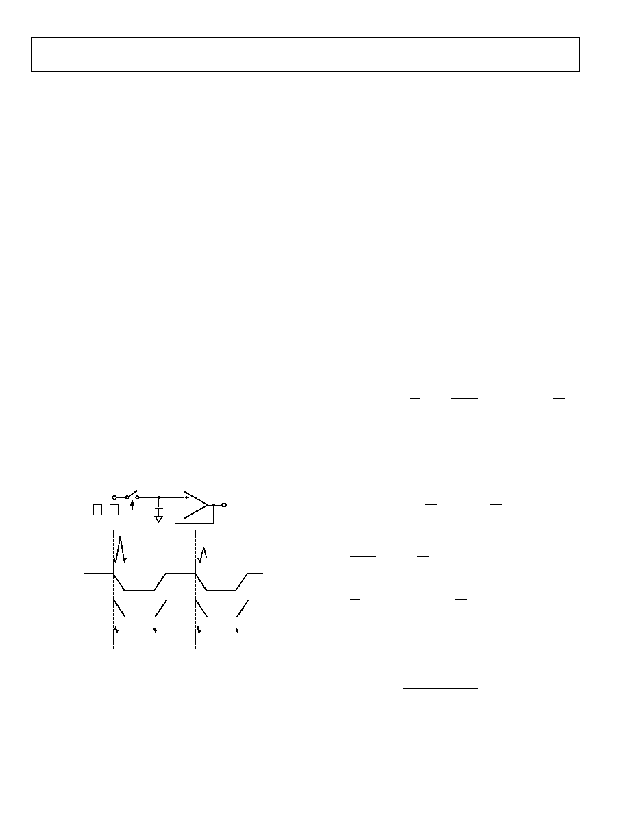
GLITCH
Worst-case glitch occurs at the transition between Half-Scale
Digital Code 1000 0000 0000 to half-scale minus 1 LSB, 0111
1111 1111. It can be measured at about 2 V μs (see Figure 36).
For demanding applications such as waveform generation or
precision instrumentation control, a deglitcher circuit can be
implemented with a standard sample-and-hold circuit (see
Figure 37). When CS is enabled by synchronizing the hold
period to be longer than the glitch tradition, the output voltage
can be smoothed with minimum disturbance. A quad
sample-and-hold amplifier, SMP04, has been used to illustrate
the deglitching result (see
).
S/H
CS
DACOUT1
DACOUT
DACOUT1
S/H
HS
H
00
27
4
-03
8
S
Figure 37. Data Output (Read Timing)
REFERENCE INPUTS
All four DACs share common reference high (VREFH) and reference
low (VREFL) inputs. The voltages applied to these reference inputs set
the output high and low voltage limits of all four of the DACs.
Each reference input has voltage restrictions with respect to the
other reference and to the power supplies. The VREFL can be set at
any voltage between VSS and VREFH 2.5 V, and VREFH can be set to
any value between +VDD 2.5 V and VREFL + 2.5 V. Note that
because of these restrictions, the DAC8412 references cannot be
inverted (that is, VREFL cannot be greater than VREFH).
It is important to note that the DAC8412 VREFH input both sinks
and sources current. In addition, the input current of both VREFH
and VREFL are code-dependent. Many references have limited
current-sinking capability and must be buffered with an
amplifier to drive VREFH. The VREFL has no such special
requirements.
It is recommended that the reference inputs be bypassed with
0.2 μF capacitors when operating with ±10 V references. This
limits the reference bandwidth.
DIGITAL I/O
See Table 6 for the digital control logic truth table. Digital I/O
consists of a 12-bit bidirectional data bus, two registers select
inputs, A0 and A1, a R/W input, a RESET input, a chip select (CS),
and a load DAC (LDAC) input. Control of the DACs and bus
direction is determined by these inputs as shown in
Digital
data bits are labeled with the MSB defined as Data Bit 11 and the
LSB as Data Bit 0. All digital pins are TTL/CMOS compatible.
See Figure 38 for a simplified I/O logic diagram. The register
select inputs A0 and A1 select individual DAC registers A
(Binary Code 00) through D (Binary Code 11). Decoding of the
registers is enabled by the CS input. When CS is high, no
decoding takes place, and neither the writing nor the reading of
the input registers is enabled. The loading of the second bank of
registers is controlled by the asynchronous LDAC input. By
taking LDAC low while CS is enabled, all output registers can
be updated simultaneously. Note that the tLDW required pulse
width for updating all DACs is a minimum of 170 ns.
The R/W input, when enabled by CS, controls the writing to
and reading from the input register.
CODING
Both DAC8412/DAC8413 use binary coding. The output
voltage can be calculated by
4096
)
(
N
V
REFL
REFH
REFL
OUT
×
+
=
where N is the digital code in decimal.
相关PDF资料 |
PDF描述 |
|---|---|
| DAC8501E/250G4 | SERIAL INPUT LOADING, 12 us SETTLING TIME, 16-BIT DAC, PDSO8 |
| DAC8551IADGKR | SERIAL INPUT LOADING, 12 us SETTLING TIME, 16-BIT DAC, PDSO8 |
| DAC8551IADGKTG4 | SERIAL INPUT LOADING, 12 us SETTLING TIME, 16-BIT DAC, PDSO8 |
| DAC8551IADGKT | SERIAL INPUT LOADING, 12 us SETTLING TIME, 16-BIT DAC, PDSO8 |
| DAC8551IADGKRG4 | SERIAL INPUT LOADING, 12 us SETTLING TIME, 16-BIT DAC, PDSO8 |
相关代理商/技术参数 |
参数描述 |
|---|---|
| DAC8413FPZ | 功能描述:IC DAC 12BIT QUAD V-OUT 28DIP RoHS:是 类别:集成电路 (IC) >> 数据采集 - 数模转换器 系列:- 标准包装:1 系列:- 设置时间:4.5µs 位数:12 数据接口:串行,SPI? 转换器数目:1 电压电源:单电源 功率耗散(最大):- 工作温度:-40°C ~ 125°C 安装类型:表面贴装 封装/外壳:8-SOIC(0.154",3.90mm 宽) 供应商设备封装:8-SOICN 包装:剪切带 (CT) 输出数目和类型:1 电压,单极;1 电压,双极 采样率(每秒):* 其它名称:MCP4921T-E/SNCTMCP4921T-E/SNRCTMCP4921T-E/SNRCT-ND |
| dac8413ft | 制造商:Rochester Electronics LLC 功能描述:- Bulk 制造商:Analog Devices 功能描述: |
| DAC8413FTC | 制造商:未知厂家 制造商全称:未知厂家 功能描述:12-Bit Digital-to-Analog Converter |
| DAC8420 | 制造商:AD 制造商全称:Analog Devices 功能描述:Quad 12-Bit Serial Voltage Output DAC |
| DAC8420_07 | 制造商:AD 制造商全称:Analog Devices 功能描述:Quad 12-Bit Serial Voltage Output DAC |
发布紧急采购,3分钟左右您将得到回复。