参数资料
| 型号: | DAC8420EPZ |
| 厂商: | Analog Devices Inc |
| 文件页数: | 6/24页 |
| 文件大小: | 0K |
| 描述: | IC DAC 12BIT QUAD SRL-OUT 16DIP |
| 产品培训模块: | Data Converter Fundamentals DAC Architectures |
| 标准包装: | 1 |
| 设置时间: | 8µs |
| 位数: | 12 |
| 数据接口: | 串行 |
| 转换器数目: | 4 |
| 电压电源: | 双 ± |
| 功率耗散(最大): | 255mW |
| 工作温度: | -40°C ~ 85°C |
| 安装类型: | 通孔 |
| 封装/外壳: | 16-DIP(0.300",7.62mm) |
| 供应商设备封装: | 16-PDIP |
| 包装: | 管件 |
| 输出数目和类型: | 4 电压,单极;4 电压,双极 |
| 采样率(每秒): | 125k |
DAC8420
Rev. B | Page 14 of 24
THEORY OF OPERATION
INTRODUCTION
The DAC8420 is a quad, voltage-output 12-bit DAC with a serial
digital input capable of operating from a single 5 V supply. The
straightforward serial interface can be connected directly to
most popular microprocessors and microcontrollers, and can
accept data at a 10 MHz clock rate when operating from ±15 V
supplies. A unique voltage reference structure ensures maximum
utilization of the DAC output resolution by allowing the user to
set the zero-scale and full-scale output levels within the supply
rails. The analog voltage outputs are fully buffered, and are
capable of driving a 2 kΩ load. Output glitch impulse during
major code transitions is a very low 64 nV-s (typ).
DIGITAL INTERFACE OPERATION
The serial input of the DAC8420, consisting of CS, SDI, and
LD, is easily interfaced to a wide variety of microprocessor serial
ports. While CS is low, the data presented to the input SDI is
shifted into the internal serial-to-parallel shift register on the
rising edge of the clock, with the address MSB first, data LSB
last, as shown in Table 6 and in the timing diagram (Figure 2).
The data format, shown in Table 8, is two bits of DAC address
and two don’t care fill bits, followed by the 12-bit DAC data-
word. Once all 16 bits of the serial data-word have been input,
the load control LD is strobed and the word is parallel-shifted
out onto the internal data bus. The two address bits are decoded
and used to route the 12-bit data-word to the appropriate DAC
data register (see the Applications section).
CORRECT OPERATION OF CS AND CLK
In Table 6, the control pins CLK and CS require some attention
during a data load cycle. Since these two inputs are fed to the
same logical OR gate, the operation is in fact identical. The user
must take care to operate them accordingly to avoid clocking in
false data bits. In the timing diagram, CLK must be halted high
or CS must be brought high during the last high portion of the
CLK following the rising edge that latched in the last data bit.
Otherwise, an additional rising edge is generated by CS rising
while CLK is low, causing CS to act as the clock and allowing a
false data bit into the serial input register. The same issue must
also be considered in the beginning of the data load sequence.
USING CLR AND CLSEL
The clear (CLR) control allows the user to perform an asyn-
chronous reset function. Asserting CLR loads all four DAC
data-word registers, forcing the DAC outputs to either zero
scale (0x000) or midscale (0x800), depending on the state of
CLSEL as shown in Table 6. The clear function is asynchronous
and totally independent of CS. When CLR returns high, the
DAC outputs remain latched at the reset value until LD is
strobed, reloading the individual DAC data-word registers
with either the data held in the serial input register prior to the
reset or with new data loaded through the serial interface.
Table 7. DAC Address Word Decode Table
A1
A0
DAC Addressed
0
DAC A
0
1
DAC B
1
0
DAC C
1
DAC D
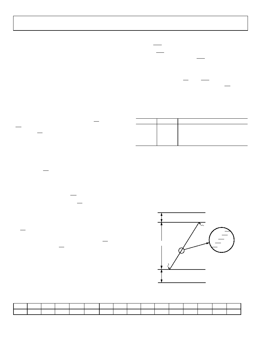
PROGRAMMING THE ANALOG OUTPUTS
The unique differential reference structure of the DAC8420
allows the user to tailor the output voltage range precisely to
the needs of the application. Instead of spending DAC resolu-
tion on an unused region near the positive or negative rail, the
DAC8420 allows the user to determine both the upper and
lower limits of the analog output voltage range. Thus, as shown
range between VREFHI and VREFLO, within the limits specified
in the Specifications section. Note also that VREFHI must be
greater than VREFLO.
1 LSB
2.5V MIN
0V MIN
VDD
VVREFHI
VVREFLO
VSS
–10V MIN
2.5V MIN
0x000
0xFFF
00
27
5-
0
06
Figure 30. Output Voltage Range Programming
Table 8.
(FIRST)
(LAST)
B0
B1
B2
B3
B4
B5
B6
B7
B8
B9
B10
B11
B12
B13
B14
B15
A1
A0
NC
D11
D10
D9
D8
D7
D6
D5
D4
D3
D2
D1
D0
—Address Word—
(MSB)
—DAC Data-Word—
(LSB)
相关PDF资料 |
PDF描述 |
|---|---|
| MS27508E18A35A | CONN HSG RCPT 66POS BOX MT PIN |
| VE-J60-MZ-S | CONVERTER MOD DC/DC 5V 25W |
| GTC030-28-12SLC | CONN HSG RCPT 26POS PNL MT SCKT |
| VI-212-MY-F1 | CONVERTER MOD DC/DC 15V 50W |
| DAC8420ESZ | IC DAC 12BIT QUAD SRL-OUT 16SOIC |
相关代理商/技术参数 |
参数描述 |
|---|---|
| DAC8420EPZ2 | 制造商:AD 制造商全称:Analog Devices 功能描述:Quad 12-Bit Serial Voltage Output DAC |
| DAC8420EQ | 制造商:Rochester Electronics LLC 功能描述:QUAD VOLT-OUTPUT 12-BIT - Bulk |
| DAC8420ES | 功能描述:IC DAC 12BIT QUAD SRL-OUT 16SOIC RoHS:否 类别:集成电路 (IC) >> 数据采集 - 数模转换器 系列:- 产品培训模块:Lead (SnPb) Finish for COTS Obsolescence Mitigation Program 标准包装:1,000 系列:- 设置时间:1µs 位数:8 数据接口:串行 转换器数目:8 电压电源:双 ± 功率耗散(最大):941mW 工作温度:0°C ~ 70°C 安装类型:表面贴装 封装/外壳:24-SOIC(0.295",7.50mm 宽) 供应商设备封装:24-SOIC W 包装:带卷 (TR) 输出数目和类型:8 电压,单极 采样率(每秒):* |
| DAC8420ES-REEL | 功能描述:IC DAC 12BIT QUAD SRL LP 16-SOIC RoHS:否 类别:集成电路 (IC) >> 数据采集 - 数模转换器 系列:- 产品培训模块:Lead (SnPb) Finish for COTS Obsolescence Mitigation Program 标准包装:1,000 系列:- 设置时间:1µs 位数:8 数据接口:串行 转换器数目:8 电压电源:双 ± 功率耗散(最大):941mW 工作温度:0°C ~ 70°C 安装类型:表面贴装 封装/外壳:24-SOIC(0.295",7.50mm 宽) 供应商设备封装:24-SOIC W 包装:带卷 (TR) 输出数目和类型:8 电压,单极 采样率(每秒):* |
| DAC8420ESZ | 功能描述:IC DAC 12BIT QUAD SRL-OUT 16SOIC RoHS:是 类别:集成电路 (IC) >> 数据采集 - 数模转换器 系列:- 标准包装:1 系列:- 设置时间:4.5µs 位数:12 数据接口:串行,SPI? 转换器数目:1 电压电源:单电源 功率耗散(最大):- 工作温度:-40°C ~ 125°C 安装类型:表面贴装 封装/外壳:8-SOIC(0.154",3.90mm 宽) 供应商设备封装:8-SOICN 包装:剪切带 (CT) 输出数目和类型:1 电压,单极;1 电压,双极 采样率(每秒):* 其它名称:MCP4921T-E/SNCTMCP4921T-E/SNRCTMCP4921T-E/SNRCT-ND |
发布紧急采购,3分钟左右您将得到回复。