参数资料
| 型号: | DAC8420EPZ |
| 厂商: | Analog Devices Inc |
| 文件页数: | 9/24页 |
| 文件大小: | 0K |
| 描述: | IC DAC 12BIT QUAD SRL-OUT 16DIP |
| 产品培训模块: | Data Converter Fundamentals DAC Architectures |
| 标准包装: | 1 |
| 设置时间: | 8µs |
| 位数: | 12 |
| 数据接口: | 串行 |
| 转换器数目: | 4 |
| 电压电源: | 双 ± |
| 功率耗散(最大): | 255mW |
| 工作温度: | -40°C ~ 85°C |
| 安装类型: | 通孔 |
| 封装/外壳: | 16-DIP(0.300",7.62mm) |
| 供应商设备封装: | 16-PDIP |
| 包装: | 管件 |
| 输出数目和类型: | 4 电压,单极;4 电压,双极 |
| 采样率(每秒): | 125k |
DAC8420
Rev. B | Page 17 of 24
APPLICATIONS
POWER SUPPLY BYPASSING AND GROUNDING
In any circuit where accuracy is important, careful consid-
eration of the power supply and ground return layout helps
to ensure the rated performance. The DAC8420 has a single
ground pin that is internally connected to the digital section
as the logic reference level. The first thought may be to connect
this pin to digital ground; however, in large systems digital
ground is often noisy because of the switching currents of other
digital circuitry. Any noise that is introduced at the ground pin
can couple into the analog output. Thus, to avoid error-causing
digital noise in the sensitive analog circuitry, the ground pin
should be connected to the system analog ground. The ground
path (circuit board trace) should be as wide as possible to reduce
any effects of parasitic inductance and ohmic drops. A ground
plane is recommended if possible. The noise immunity of the
on-board digital circuitry, typically in the hundreds of milli-
volts, is well able to reject the common-mode noise typically
seen between system analog and digital grounds. Finally, the
analog and digital ground should be connected to each other
at a single point in the system to provide a common reference.
This is preferably done at the power supply.
Good grounding practice is also essential to maintaining analog
performance in the surrounding analog support circuitry. With
two reference inputs and four analog outputs capable of moderate
bandwidth and output current, there is a significant potential
for ground loops. Again, a ground plane is recommended as the
most effective solution to minimizing errors due to noise and
ground offsets.
00
27
5-
0
31
VDD
VSS
GND
+VS
–VS
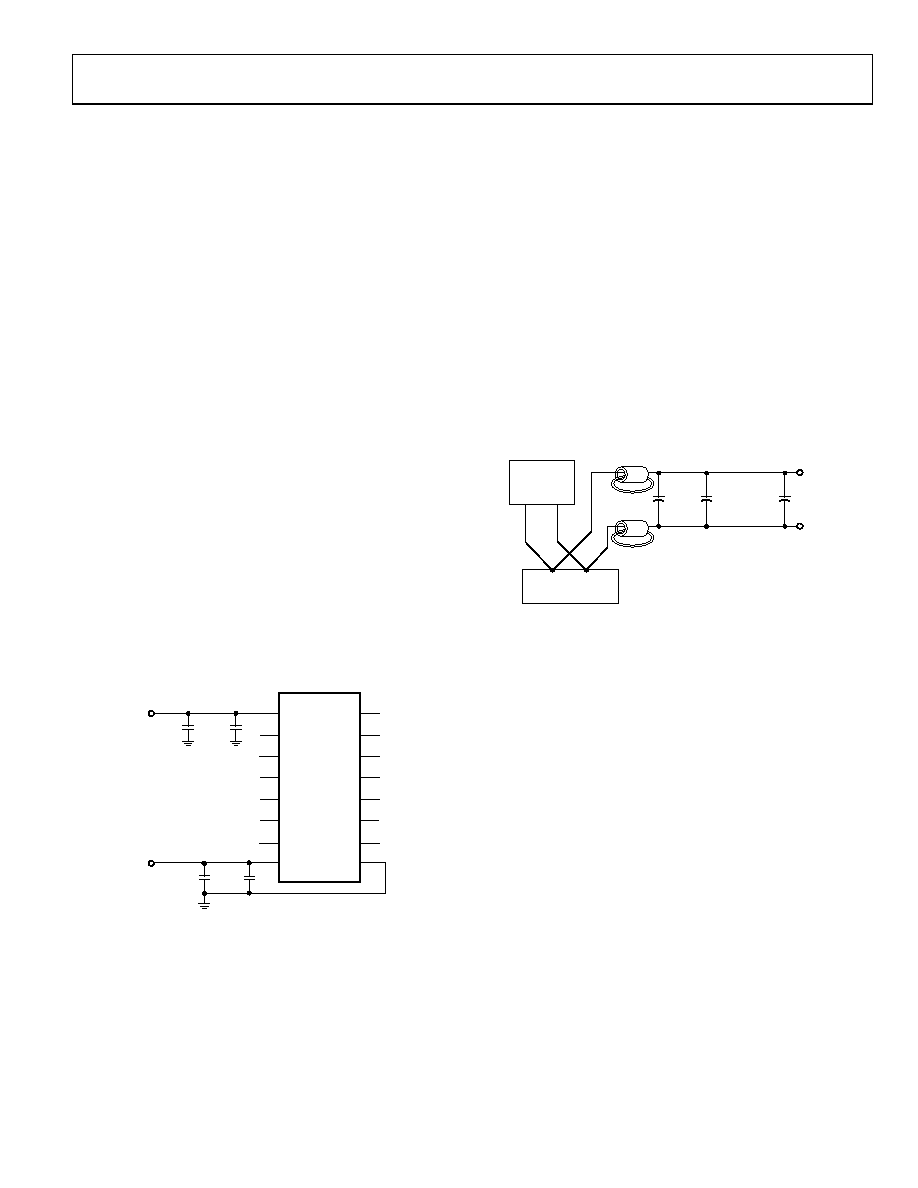
10F
0.1F
10F
0.1F
1
89
10F = TANTALUM
0.1F = CERAMIC
Figure 31. Recommended Supply Bypassing Scheme
The DAC8420 should have ample supply bypassing, located as
close to the package as possible. Figure 31 shows the recom-
mended capacitor values of 10 μF in parallel with 0.1 μF. The
0.1 μF capacitor should have low effective series resistance (ESR)
and effective series inductance (ESI) (such as any common
ceramic type capacitor), which provide a low impedance path
to ground at high frequencies to handle transient currents due
to internal logic switching. To preserve the specified analog
performance of the device, the supply should be as noise free as
possible. In the case of 5 V only systems, it is desirable to use
the same 5 V supply for both the analog circuitry and the
digital portion of the circuit. Unfortunately, the typical 5 V
supply is extremely noisy due to the fast edge rates of the
popular CMOS logic families, which induce large inductive
voltage spikes, and busy microcontroller or microprocessor
buses, and therefore commonly have large current spikes during
bus activity. However, by properly filtering the supply as shown
in Figure 32, the digital 5 V supply can be used. The inductors
and capacitors generate a filter that not only rejects noise due
to the digital circuitry, but also filters out the lower frequency
noise of switch mode power supplies. The analog supply should
be connected as close as possible to the origin of the digital
supply to minimize noise pickup from the digital section.
+
TTL/CMOS
LOGIC
CIRCUITS
+5V
POWER SUPPLY
FERRITE BEADS:
2 TURNS, FAIR-RITE
#2677006301
100F
ELECT.
10F TO 22F
TANT.
0.1F
CER.
+5V
RETURN
00
27
5-
0
32
Figure 32. Single-Supply Analog Supply Filter
ANALOG OUTPUTS
The DAC8420 features buffered analog voltage outputs capable
of sourcing and sinking up to 5 mA when operating from ±15 V
supplies, eliminating the need for external buffer amplifiers in
most applications while maintaining specified accuracy over the
rated operating conditions. The buffered outputs are simply an
op amp connected as a voltage follower, and thus have output
characteristics very similar to the typical operational amplifier.
These amplifiers are short-circuit protected. The user should
verify that the output load meets the capabilities of the device,
in terms of both output current and load capacitance. The
DAC8420 is stable with capacitive loads up to 2 nF typically.
However, any capacitive load will increase the settling time,
and should be minimized if speed is a concern.
The output stage includes a P-channel MOSFET to pull the
output voltage down to the negative supply. This is very important
in single-supply systems where VREFLO usually has the same
potential as the negative supply. With no load, the zero-scale
output voltage in these applications is less than 500 μV typically,
or less than 1 LSB when VVREFHI = 2.5 V. However, when sinking
current, this voltage does increase because of the finite imped-
ance of the output stage. The effective value of the pull-down
resistor in the output stage is typically 320 Ω. With a 100 kΩ
resistor connected to 5 V, the resulting zero-scale output voltage
相关PDF资料 |
PDF描述 |
|---|---|
| MS27508E18A35A | CONN HSG RCPT 66POS BOX MT PIN |
| VE-J60-MZ-S | CONVERTER MOD DC/DC 5V 25W |
| GTC030-28-12SLC | CONN HSG RCPT 26POS PNL MT SCKT |
| VI-212-MY-F1 | CONVERTER MOD DC/DC 15V 50W |
| DAC8420ESZ | IC DAC 12BIT QUAD SRL-OUT 16SOIC |
相关代理商/技术参数 |
参数描述 |
|---|---|
| DAC8420EPZ2 | 制造商:AD 制造商全称:Analog Devices 功能描述:Quad 12-Bit Serial Voltage Output DAC |
| DAC8420EQ | 制造商:Rochester Electronics LLC 功能描述:QUAD VOLT-OUTPUT 12-BIT - Bulk |
| DAC8420ES | 功能描述:IC DAC 12BIT QUAD SRL-OUT 16SOIC RoHS:否 类别:集成电路 (IC) >> 数据采集 - 数模转换器 系列:- 产品培训模块:Lead (SnPb) Finish for COTS Obsolescence Mitigation Program 标准包装:1,000 系列:- 设置时间:1µs 位数:8 数据接口:串行 转换器数目:8 电压电源:双 ± 功率耗散(最大):941mW 工作温度:0°C ~ 70°C 安装类型:表面贴装 封装/外壳:24-SOIC(0.295",7.50mm 宽) 供应商设备封装:24-SOIC W 包装:带卷 (TR) 输出数目和类型:8 电压,单极 采样率(每秒):* |
| DAC8420ES-REEL | 功能描述:IC DAC 12BIT QUAD SRL LP 16-SOIC RoHS:否 类别:集成电路 (IC) >> 数据采集 - 数模转换器 系列:- 产品培训模块:Lead (SnPb) Finish for COTS Obsolescence Mitigation Program 标准包装:1,000 系列:- 设置时间:1µs 位数:8 数据接口:串行 转换器数目:8 电压电源:双 ± 功率耗散(最大):941mW 工作温度:0°C ~ 70°C 安装类型:表面贴装 封装/外壳:24-SOIC(0.295",7.50mm 宽) 供应商设备封装:24-SOIC W 包装:带卷 (TR) 输出数目和类型:8 电压,单极 采样率(每秒):* |
| DAC8420ESZ | 功能描述:IC DAC 12BIT QUAD SRL-OUT 16SOIC RoHS:是 类别:集成电路 (IC) >> 数据采集 - 数模转换器 系列:- 标准包装:1 系列:- 设置时间:4.5µs 位数:12 数据接口:串行,SPI? 转换器数目:1 电压电源:单电源 功率耗散(最大):- 工作温度:-40°C ~ 125°C 安装类型:表面贴装 封装/外壳:8-SOIC(0.154",3.90mm 宽) 供应商设备封装:8-SOICN 包装:剪切带 (CT) 输出数目和类型:1 电压,单极;1 电压,双极 采样率(每秒):* 其它名称:MCP4921T-E/SNCTMCP4921T-E/SNRCTMCP4921T-E/SNRCT-ND |
发布紧急采购,3分钟左右您将得到回复。