参数资料
| 型号: | DAC8512FPZ |
| 厂商: | Analog Devices Inc |
| 文件页数: | 6/20页 |
| 文件大小: | 0K |
| 描述: | IC DAC 12BIT 5V COMPLETE 8-DIP |
| 产品培训模块: | Data Converter Fundamentals DAC Architectures |
| 标准包装: | 50 |
| 设置时间: | 16µs |
| 位数: | 12 |
| 数据接口: | 串行 |
| 转换器数目: | 1 |
| 电压电源: | 单电源 |
| 功率耗散(最大): | 2.5mW |
| 工作温度: | -40°C ~ 85°C |
| 安装类型: | 通孔 |
| 封装/外壳: | 8-DIP(0.300",7.62mm) |
| 供应商设备封装: | 8-PDIP |
| 包装: | 管件 |
| 输出数目和类型: | 1 电压,单极;1 电压,双极 |
| 采样率(每秒): | 62.5k |
| 产品目录页面: | 786 (CN2011-ZH PDF) |
DAC8512
–14–
REV. A
COUNTER
CLK
Q
D
Q
C
Q
B
Q
A
LOAD
(X)
DAC8512
CLK (Y)
DAC8512 CLK = LOAD
SCLK
LOAD = Q
C QD
LOAD DAC
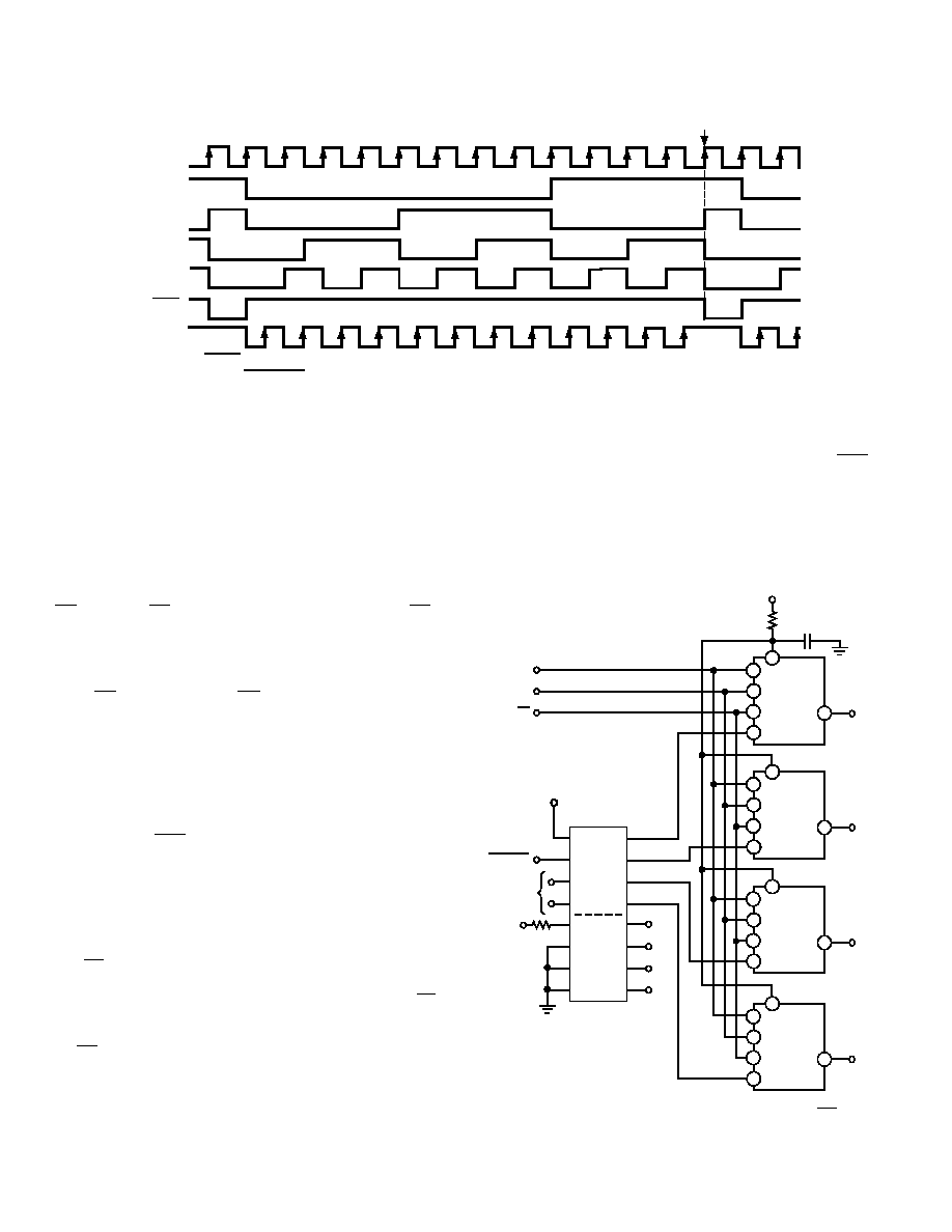
Figure 36. Opto-lsolated Two-Wire Serial Interface Timing Diagram
The timing diagram of Figure 36 can be used to understand the
operation of the circuit. Only two opto-couplers are used in the
circuit; one for SCLK and one for SDI. The 74HC161 counter
in incremented on every rising edge of the clock. Additionally,
the data is loaded into the DAC8512 on the falling edge of the
clock by inverting the serial clock using gate “Y.” The timing
diagram shows that after the twelfth bit has been clocked the
output of the counter is binary 1011. On the very next rising
clock edge, the output of the counter changes to binary 1100
upon which the output of gate “X” goes LOW to generate the
LD
pulse. The LD signal is connected to both the DAC’s LD
and the counter’s LOAD pins to prevent the thirteenth rising
clock edge from advancing the DAC’s internal shift register.
This prevents false loading of data into the DAC8512. Inverting
the DAC’s serial clock allows sufficient time from the CLK edge
to the LD edge, and from the LD edge to the next clock pulse
all of which satisfies the timing requirements for loading the
DAC8512.
After loading one address of the DAC, the entire process can re-
peated to load another address. If the loading is complete, then
the clock must stop after the thirteenth pulse of the final load.
The DAC’s clock input will be pulled high and the counter reset
to zero. As was shown in Figure 35, both the 74HC161’s and
the DAC8512’s CLR pins are connected to a simple R-C timing
circuit that resets both ICs when the power in turned on. The
circuit’s time constant should be set longer than the power sup-
ply turn-on time and, in this circuit, is set to 10 ms, which
should be adequate for most systems. This same two-wire inter-
face can be used for other three-wire serial input DACs.
Decoding Multiple DAC8512s
The CS function of the DAC8512 can be used in applications
to decode a number of DACs. In this application, all DACs re-
ceive the same input data; however, only one of the DAC’s CS
input is asserted to transfer its serial input register contents into
the destination DAC register. In this circuit, shown in Figure 37,
the CS timing is generated by a 74HC139 decoder and should
follow the DAC8512’s standard timing requirements. To pre-
vent timing errors, the 74HC139 should not be activated by its
VOUT3
DAC8512
#3
VOUT2
DAC8512
#2
VOUT1
DAC8512
#1
8
4
5
2
3
6
VCC
1G
1A
1B
2G
2A
2B
GND
1Y0
1Y1
1Y2
1Y3
2Y0
2Y1
2Y2
2Y3
12
1k
+5V
16
1
2
3
15
14
13
8
11
10
9
7
6
5
4
NC
+5V
ENABLE
CODED
ADDRESS
C1
0.1
F
74HC139
VOUT4
DAC8512
#4
+5V
R1
1k
SCLK
SDI
LD
8
4
5
2
3
6
8
4
5
2
3
6
8
4
5
2
3
6
Figure 37. Decoding Multiple DAC8512s Using the CS Pin
ENABLE input while the coded address inputs are changing. A
simple timing circuit, R1 and C1, connected to the DACs’ CLR
pins resets all DAC outputs to zero during power-up.
相关PDF资料 |
PDF描述 |
|---|---|
| LTC1658CMS8#PBF | IC D/A CONV 14BIT R-R 8-MSOP |
| ICS870931ARI-01LFT | IC CLK GENERATOR LVCMOS 20QSOP |
| ICS1562BM-001T | IC VIDEO CLK SYNTHESIZER 16-SOIC |
| AD5062BRJZ-2500RL7 | IC DAC 16BIT 2.7-5.5V SOT23-8 |
| ICS843023AGILFT | IC CLK GENERATOR LVPECL 8-TSSOP |
相关代理商/技术参数 |
参数描述 |
|---|---|
| DAC8512FS | 功能描述:IC DAC 12BIT 5V COMPLETE 8-SOIC RoHS:否 类别:集成电路 (IC) >> 数据采集 - 数模转换器 系列:- 标准包装:47 系列:- 设置时间:2µs 位数:14 数据接口:并联 转换器数目:1 电压电源:单电源 功率耗散(最大):55µW 工作温度:-40°C ~ 85°C 安装类型:表面贴装 封装/外壳:28-SSOP(0.209",5.30mm 宽) 供应商设备封装:28-SSOP 包装:管件 输出数目和类型:1 电流,单极;1 电流,双极 采样率(每秒):* |
| DAC8512FS-REEL | 制造商:Analog Devices 功能描述:DAC 1-CH R-2R 12-bit 8-Pin SOIC N T/R |
| DAC8512FS-REEL7 | 功能描述:IC DAC 12BIT SRL LP 5V 8-SOIC RoHS:否 类别:集成电路 (IC) >> 数据采集 - 数模转换器 系列:- 标准包装:47 系列:- 设置时间:2µs 位数:14 数据接口:并联 转换器数目:1 电压电源:单电源 功率耗散(最大):55µW 工作温度:-40°C ~ 85°C 安装类型:表面贴装 封装/外壳:28-SSOP(0.209",5.30mm 宽) 供应商设备封装:28-SSOP 包装:管件 输出数目和类型:1 电流,单极;1 电流,双极 采样率(每秒):* |
| DAC8512FSZ | 功能描述:IC DAC 12BIT 5V COMPLETE 8-SOIC RoHS:是 类别:集成电路 (IC) >> 数据采集 - 数模转换器 系列:- 产品培训模块:Lead (SnPb) Finish for COTS Obsolescence Mitigation Program 标准包装:50 系列:- 设置时间:4µs 位数:12 数据接口:串行 转换器数目:2 电压电源:单电源 功率耗散(最大):- 工作温度:-40°C ~ 85°C 安装类型:表面贴装 封装/外壳:8-TSSOP,8-MSOP(0.118",3.00mm 宽) 供应商设备封装:8-uMAX 包装:管件 输出数目和类型:2 电压,单极 采样率(每秒):* 产品目录页面:1398 (CN2011-ZH PDF) |
| DAC8512FSZ-REEL | 功能描述:IC DAC 12BIT SRL LP 5V 8SOIC RoHS:是 类别:集成电路 (IC) >> 数据采集 - 数模转换器 系列:- 产品培训模块:LTC263x 12-, 10-, and 8-Bit VOUT DAC Family 特色产品:LTC2636 - Octal 12-/10-/8-Bit SPI VOUT DACs with 10ppm/°C Reference 标准包装:91 系列:- 设置时间:4µs 位数:10 数据接口:MICROWIRE?,串行,SPI? 转换器数目:8 电压电源:单电源 功率耗散(最大):2.7mW 工作温度:-40°C ~ 85°C 安装类型:表面贴装 封装/外壳:14-WFDFN 裸露焊盘 供应商设备封装:14-DFN-EP(4x3) 包装:管件 输出数目和类型:8 电压,单极 采样率(每秒):* |
发布紧急采购,3分钟左右您将得到回复。