参数资料
| 型号: | DAC8512FPZ |
| 厂商: | Analog Devices Inc |
| 文件页数: | 7/20页 |
| 文件大小: | 0K |
| 描述: | IC DAC 12BIT 5V COMPLETE 8-DIP |
| 产品培训模块: | Data Converter Fundamentals DAC Architectures |
| 标准包装: | 50 |
| 设置时间: | 16µs |
| 位数: | 12 |
| 数据接口: | 串行 |
| 转换器数目: | 1 |
| 电压电源: | 单电源 |
| 功率耗散(最大): | 2.5mW |
| 工作温度: | -40°C ~ 85°C |
| 安装类型: | 通孔 |
| 封装/外壳: | 8-DIP(0.300",7.62mm) |
| 供应商设备封装: | 8-PDIP |
| 包装: | 管件 |
| 输出数目和类型: | 1 电压,单极;1 电压,双极 |
| 采样率(每秒): | 62.5k |
| 产品目录页面: | 786 (CN2011-ZH PDF) |
DAC8512
–15–
REV. A
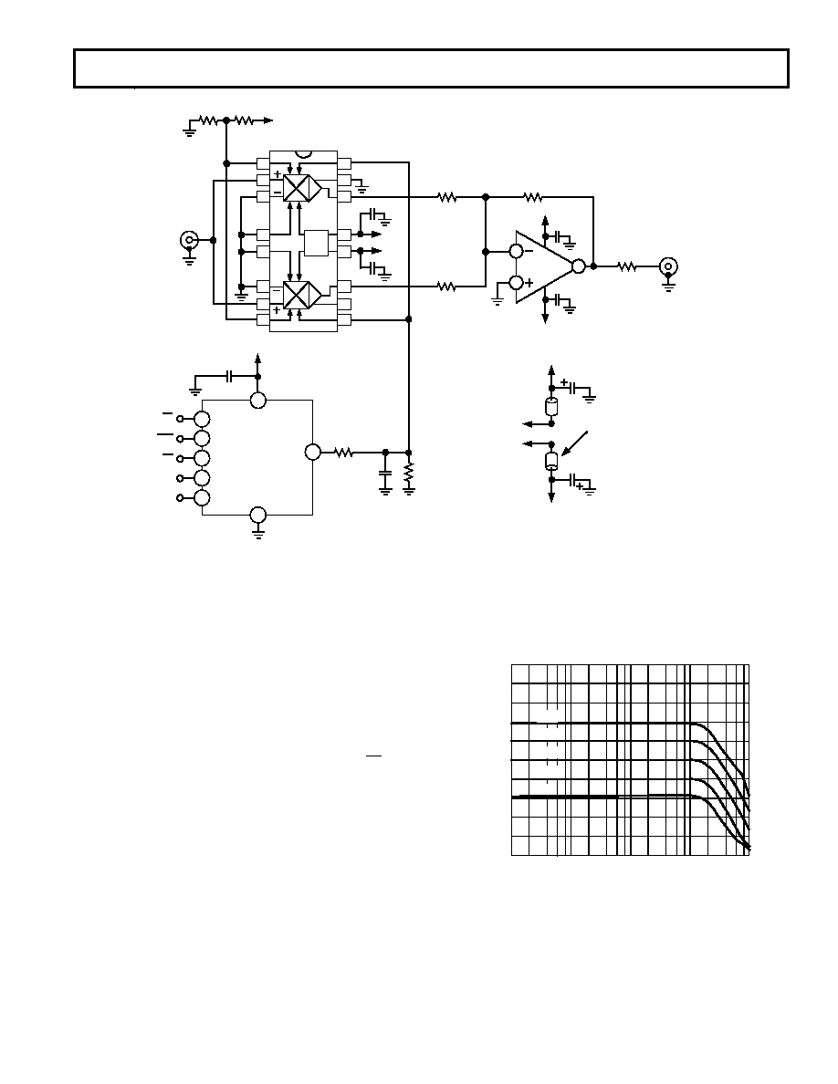
A Digitally Controlled, Ultralow Noise VCA
The circuit in Figure 38 illustrates how the DAC8512 can be
used to control an ultralow noise VCA, using the AD600/
AD602. The AD600/AD602 is a dual, low noise, wideband,
variable gain amplifier based on the X-AMP topology.* Both
channels of the AD600 are wired in parallel to achieve a
wideband VCA which exhibits an RTI (Referred To Input)
noise voltage spectral density of approximately 1 nV/
√Hz. The
output of the VCA requires an AD844 configured in a gain of 4
to account for signal loss due to input and output 50
termina-
tions. As configured, the total gain in the circuit is 40 dB.
Since the output of the DAC8512 is single quadrant, it was nec-
essary to offset the AD600’s gain control voltage so that the gain
of the circuit is 0 dB for zero scale and 40 dB at full scale. This
was achieved by setting C1LO and C2LO to +625 mV using R1
and R2. Next, the output of the DAC8512 was scaled so that
the gain of the AD600 equaled 20 dB when the digital input
code equaled 800H. The frequency response of the VCA as a
function of digital code is shown in Figure 39.
*For more details regarding the AD600 or AD602, please consult the AD600/
AD602 data sheet.
+70
+20
–30
100k
100M
10M
1M
10k
+30
+40
+50
+60
–20
–10
0
+10
FREQUENCY – Hz
SYSTEM
GAIN
–
dB
4095
3072
2048
1024
0
Figure 39. VCA Frequency Response vs. Digital Code
1
2
3
4
5
6
7
8
16
15
14
13
12
11
10
9
REF
AD600JN
V+
V–
0.1
F
0.1
F
6
2
DAC8512FZ
8
7
CS
CLR
1
0.1
F
V+
1
F
R6
2.26k
R7
1k
0
≤ V
G ≤ 1.25V
5
LD
3
SCLK
4
SDI
R1
619
R2
4.32k
V+
+625mV
6
3
2
0.1
F
0.1
F
V+
V
OUT
0.01dB/BIT
10
F
+5V
10
F
–5V
V+
V–
FB = FAIR RITE
#2743001111
SUPPLY DECOUPLING NETWORK
V–
R5
806
R3
402
R4
402
R4
49.9
V
IN
AD844
Figure 38. A Digitally Controlled, Ultralow Noise VCA
相关PDF资料 |
PDF描述 |
|---|---|
| LTC1658CMS8#PBF | IC D/A CONV 14BIT R-R 8-MSOP |
| ICS870931ARI-01LFT | IC CLK GENERATOR LVCMOS 20QSOP |
| ICS1562BM-001T | IC VIDEO CLK SYNTHESIZER 16-SOIC |
| AD5062BRJZ-2500RL7 | IC DAC 16BIT 2.7-5.5V SOT23-8 |
| ICS843023AGILFT | IC CLK GENERATOR LVPECL 8-TSSOP |
相关代理商/技术参数 |
参数描述 |
|---|---|
| DAC8512FS | 功能描述:IC DAC 12BIT 5V COMPLETE 8-SOIC RoHS:否 类别:集成电路 (IC) >> 数据采集 - 数模转换器 系列:- 标准包装:47 系列:- 设置时间:2µs 位数:14 数据接口:并联 转换器数目:1 电压电源:单电源 功率耗散(最大):55µW 工作温度:-40°C ~ 85°C 安装类型:表面贴装 封装/外壳:28-SSOP(0.209",5.30mm 宽) 供应商设备封装:28-SSOP 包装:管件 输出数目和类型:1 电流,单极;1 电流,双极 采样率(每秒):* |
| DAC8512FS-REEL | 制造商:Analog Devices 功能描述:DAC 1-CH R-2R 12-bit 8-Pin SOIC N T/R |
| DAC8512FS-REEL7 | 功能描述:IC DAC 12BIT SRL LP 5V 8-SOIC RoHS:否 类别:集成电路 (IC) >> 数据采集 - 数模转换器 系列:- 标准包装:47 系列:- 设置时间:2µs 位数:14 数据接口:并联 转换器数目:1 电压电源:单电源 功率耗散(最大):55µW 工作温度:-40°C ~ 85°C 安装类型:表面贴装 封装/外壳:28-SSOP(0.209",5.30mm 宽) 供应商设备封装:28-SSOP 包装:管件 输出数目和类型:1 电流,单极;1 电流,双极 采样率(每秒):* |
| DAC8512FSZ | 功能描述:IC DAC 12BIT 5V COMPLETE 8-SOIC RoHS:是 类别:集成电路 (IC) >> 数据采集 - 数模转换器 系列:- 产品培训模块:Lead (SnPb) Finish for COTS Obsolescence Mitigation Program 标准包装:50 系列:- 设置时间:4µs 位数:12 数据接口:串行 转换器数目:2 电压电源:单电源 功率耗散(最大):- 工作温度:-40°C ~ 85°C 安装类型:表面贴装 封装/外壳:8-TSSOP,8-MSOP(0.118",3.00mm 宽) 供应商设备封装:8-uMAX 包装:管件 输出数目和类型:2 电压,单极 采样率(每秒):* 产品目录页面:1398 (CN2011-ZH PDF) |
| DAC8512FSZ-REEL | 功能描述:IC DAC 12BIT SRL LP 5V 8SOIC RoHS:是 类别:集成电路 (IC) >> 数据采集 - 数模转换器 系列:- 产品培训模块:LTC263x 12-, 10-, and 8-Bit VOUT DAC Family 特色产品:LTC2636 - Octal 12-/10-/8-Bit SPI VOUT DACs with 10ppm/°C Reference 标准包装:91 系列:- 设置时间:4µs 位数:10 数据接口:MICROWIRE?,串行,SPI? 转换器数目:8 电压电源:单电源 功率耗散(最大):2.7mW 工作温度:-40°C ~ 85°C 安装类型:表面贴装 封装/外壳:14-WFDFN 裸露焊盘 供应商设备封装:14-DFN-EP(4x3) 包装:管件 输出数目和类型:8 电压,单极 采样率(每秒):* |
发布紧急采购,3分钟左右您将得到回复。