- 您现在的位置:买卖IC网 > PDF目录295418 > DAC902U PARALLEL, WORD INPUT LOADING, 0.03 us SETTLING TIME, 12-BIT DAC, PDSO28 PDF资料下载
参数资料
| 型号: | DAC902U |
| 元件分类: | DAC |
| 英文描述: | PARALLEL, WORD INPUT LOADING, 0.03 us SETTLING TIME, 12-BIT DAC, PDSO28 |
| 封装: | SO-28 |
| 文件页数: | 5/16页 |
| 文件大小: | 216K |
| 代理商: | DAC902U |
13
DAC902
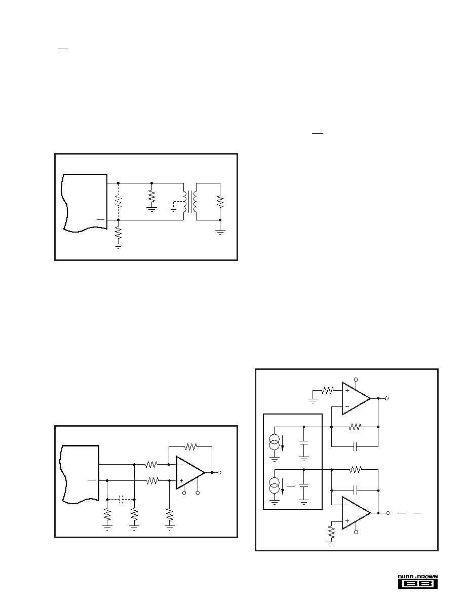
As shown in Figure 3, the transformer’s center tap is con-
nected to ground. This forces the voltage swing on IOUT and
IOUT to be centered at 0V. In this case the two resistors, RS,
may be replaced with one, RDIFF, or omitted altogether. This
approach should only be used if all components are close to
each other, and if the VSWR is not important. A complete
power transfer from the DAC output to the load can be
realized, but the output compliance range should be ob-
served. Alternatively, if the center tap is not connected, the
signal swing will be centered at RS IOUTFS/2. However, in
this case, the two resistors, RS, must be used to enable the
necessary dc-current flow for both outputs.
The OPA680 is configured for a gain of two. Therefore,
operating the DAC902 with a 20mA full-scale output will
produce a voltage output of
±1V. This requires the amplifier
to operate off of a dual power supply (
±5V). The tolerance
of the resistors typically sets the limit for the achievable
common-mode rejection. An improvement can be obtained
by fine tuning resistor R4.
This configuration typically delivers a lower level of ac
performance than the previously discussed transformer solu-
tion because the amplifier introduces another source of
distortion. Suitable amplifiers should be selected based on
their slew-rate, harmonic distortion, and output swing capa-
bilities. High-speed amplifiers like the OPA680 or OPA687
may be considered. The ac performance of this circuit may
be improved by adding a small capacitor, CDIFF, between the
outputs IOUT and IOUT (see Figure 4). This will introduce a
real pole to create a low-pass filter in order to slew-limiting
the DACs fast output signal steps, which otherwise could
drive the amplifier into slew-limitations or into an overload
condition; both would cause excessive distortion. The differ-
ence amplifier can easily be modified to add a level shift for
applications requiring the single-ended output voltage to be
unipolar, i.e., swing between 0V and +2V.
DUAL TRANSIMPEDANCE OUTPUT CONFIGURATION
The circuit example of Figure 5 shows the signal output
currents connected into the summing junction of the
OPA2680, which is set up as a transimpedance stage, or
‘I to V converter’. With this circuit, the DAC’s output will
be kept at a virtual ground, minimizing the effects of output
impedance variations, which results in the best dc linearity
(INL). However, as mentioned previously, the amplifier
may be driven into slew-rate limitations, and produce un-
wanted distortion. This may occur, especially, at high DAC
update rates.
DIFFERENTIAL CONFIGURATION USING AN OP AMP
If the application requires a dc-coupled output, a difference
amplifier may be considered, as shown in Figure 4. Four
external resistors are needed to configure the voltage-feed-
back op amp OPA680 as a difference amplifier performing
the differential to single-ended conversion. Under the shown
configuration, the DAC902 generates a differential output
signal of 0.5Vp-p at the load resistors, RL. The resistor
values shown were selected to result in a symmetric 25
loading for each of the current outputs since the input
impedance of the difference amplifier is in parallel to resis-
tors RL, and should be considered.
FIGURE 4. Difference Amplifier Provides Differential to
Single-Ended Conversion and DC-Coupling.
FIGURE 5. Dual, Voltage-Feedback Amplifier OPA2680
Forms Differential Transimpedance Amplifier.
1/2
OPA2680
1/2
OPA2680
DAC902
–V
OUT = IOUT RF
–V
OUT = IOUT RF
R
F1
R
F2
C
F1
C
F2
C
D1
C
D2
I
OUT
I
OUT
50
50
–5V
+5V
I
OUT
I
OUT
DAC902
R
L
26.1
R
L
28.7
R
4
402
R
3
200
R
2
402
R
1
200
OPA680
C
OPT
+5V
V
OUT
–5V
DAC902
I
OUT
I
OUT
1:1
ADT1-1WT
(Mini-Circuits)
R
S
50
R
S
50
R
L
Optional
R
DIFF
FIGURE 3. Differential Output Configuration Using an RF
Transformer.
相关PDF资料 |
PDF描述 |
|---|---|
| DAC908E/2K5 | PARALLEL, 8 BITS INPUT LOADING, 0.03 us SETTLING TIME, 8-BIT DAC, PDSO28 |
| DAC908U/1K | PARALLEL, 8 BITS INPUT LOADING, 0.03 us SETTLING TIME, 8-BIT DAC, PDSO28 |
| DAC908U | PARALLEL, 8 BITS INPUT LOADING, 0.03 us SETTLING TIME, 8-BIT DAC, PDSO28 |
| DAT-3175-PN | 0 MHz - 2000 MHz RF/MICROWAVE VARIABLE ATTENUATOR, 2.1 dB INSERTION LOSS-MAX |
| DA | FEMALE; MALE, D SUBMINIATURE CONNECTOR, SOLDER |
相关代理商/技术参数 |
参数描述 |
|---|---|
| DAC902U | 制造商:Texas Instruments 功能描述:12-BIT DIGITAL/ANALOG CONVERTER 12 RESO |
| DAC902U/1K | 功能描述:数模转换器- DAC 12-Bit 165MSPS SpeedPlus DAC RoHS:否 制造商:Texas Instruments 转换器数量:1 DAC 输出端数量:1 转换速率:2 MSPs 分辨率:16 bit 接口类型:QSPI, SPI, Serial (3-Wire, Microwire) 稳定时间:1 us 最大工作温度:+ 85 C 安装风格:SMD/SMT 封装 / 箱体:SOIC-14 封装:Tube |
| DAC902U/1KG4 | 功能描述:数模转换器- DAC 12-Bit 165MSPS SpeedPlus DAC RoHS:否 制造商:Texas Instruments 转换器数量:1 DAC 输出端数量:1 转换速率:2 MSPs 分辨率:16 bit 接口类型:QSPI, SPI, Serial (3-Wire, Microwire) 稳定时间:1 us 最大工作温度:+ 85 C 安装风格:SMD/SMT 封装 / 箱体:SOIC-14 封装:Tube |
| DAC902UG4 | 功能描述:数模转换器- DAC 12-Bit 165MSPS SpeedPlus DAC RoHS:否 制造商:Texas Instruments 转换器数量:1 DAC 输出端数量:1 转换速率:2 MSPs 分辨率:16 bit 接口类型:QSPI, SPI, Serial (3-Wire, Microwire) 稳定时间:1 us 最大工作温度:+ 85 C 安装风格:SMD/SMT 封装 / 箱体:SOIC-14 封装:Tube |
| DAC904 | 制造商:BB 制造商全称:BB 功能描述:14-Bit, 165MSPS DIGITAL-TO-ANALOG CONVERTER |
发布紧急采购,3分钟左右您将得到回复。