- 您现在的位置:买卖IC网 > PDF目录20383 > DC1227A (Linear Technology)BOARD EVALUATION FOR LTC3534 PDF资料下载
参数资料
| 型号: | DC1227A |
| 厂商: | Linear Technology |
| 文件页数: | 9/20页 |
| 文件大小: | 0K |
| 描述: | BOARD EVALUATION FOR LTC3534 |
| 设计资源: | DC1227A Design Files DC1227A Schematic |
| 标准包装: | 1 |
| 主要目的: | DC/DC,步升/步降 |
| 输出及类型: | 1,非隔离 |
| 输出电压: | 5V |
| 电流 - 输出: | 500mA(最小值) |
| 输入电压: | 3.6 ~ 7 V |
| 稳压器拓扑结构: | 降压-升压 |
| 频率 - 开关: | 1MHz |
| 板类型: | 完全填充 |
| 已供物品: | 板 |
| 已用 IC / 零件: | LTC3534 |
�� �
�
�LTC3534�
�OPERATION�
�The� LTC3534� provides� high� efficiency,� low� noise� power�
�for� a� wide� variety� of� handheld� electronic� devices.� Linear�
�Technology’s� proprietary� topology� allows� input� voltages�
�above,� below� or� equal� to� the� output� voltage� by� properly�
�phasing� the� output� switches.� The� error� amplifier� output�
�voltage� on� V� C� determines� the� output� duty� cycle� of� the�
�switches.� Since� V� C� is� a� filtered� signal,� it� provides� rejection�
�of� frequencies� from� well� below� the� switching� frequency.�
�The� low� R� DS(ON)� ,� low� gate� charge� synchronous� switches�
�provide� high� frequency� pulse� width� modulation� control� at�
�high� efficiency.� High� efficiency� is� achieved� at� light� loads�
�when� Burst� Mode� operation� is� invoked� and� the� LTC3534’s�
�quiescent� current� drops� to� a� mere� 25μA.�
�LOW� NOISE� FIXED� FREQUENCY� OPERATION�
�Oscillator�
�The� frequency� of� operation� is� internally� set� to� 1MHz.�
�Error� Amplifier�
�The� error� amplifier� is� a� voltage� mode� amplifier.� The� loop�
�compensation� components� are� configured� around� the�
�amplifier� (from� FB� to� V� C� )� to� obtain� stability� of� the� converter.�
�For� improved� bandwidth,� an� additional� R-C� feedforward�
�network� can� be� placed� across� the� upper� feedback� divider�
�resistor.� The� voltage� on� RUN/SS� clamps� the� error� amplifier�
�output,� V� C� ,� to� provide� a� soft-start� function.�
�Supply� Current� Limits�
�There� are� two� different� supply� current� limit� circuits� in� the�
�LTC3534,� each� having� internally� fixed� thresholds.�
�The� first� circuit� is� an� average� current� limit� amplifier,� sourc-�
�ing� current� out� of� FB� to� drop� the� output� voltage� should�
�the� peak� input� current� exceed� 1.8A� typical.� This� method�
�provides� a� closed� loop� means� of� clamping� the� input� cur-�
�rent.� During� conditions� where� V� OUT� is� near� ground,� such�
�as� during� a� short� circuit� or� start-up,� this� threshold� is� cut�
�to� 800mA� typical,� providing� a� foldback� feature.� For� this�
�current� limit� feature� to� be� most� effective,� the� Thevenin�
�resistance� from� FB� to� ground� should� be� greater� than� 100k.�
�Should� the� peak� input� current� exceed� 2.6A� typical,� the�
�second� circuit,� a� high� speed� peak� current� limit� compara-�
�tor,� shuts� off� PMOS� switch� A.� The� delay� to� output� of� this�
�comparator� is� typically� 50ns.�
�Reverse� Current� Limit�
�During� fixed� frequency� operation,� the� LTC3534� operates�
�in� forced� continuous� conduction� mode.� The� reverse� cur-�
�rent� limit� comparator� monitors� the� inductor� current� from�
�the� output� through� PMOS� switch� D.� Should� this� negative�
�inductor� current� exceed� 500mA� typical,� the� LTC3534�
�shuts� off� switch� D.�
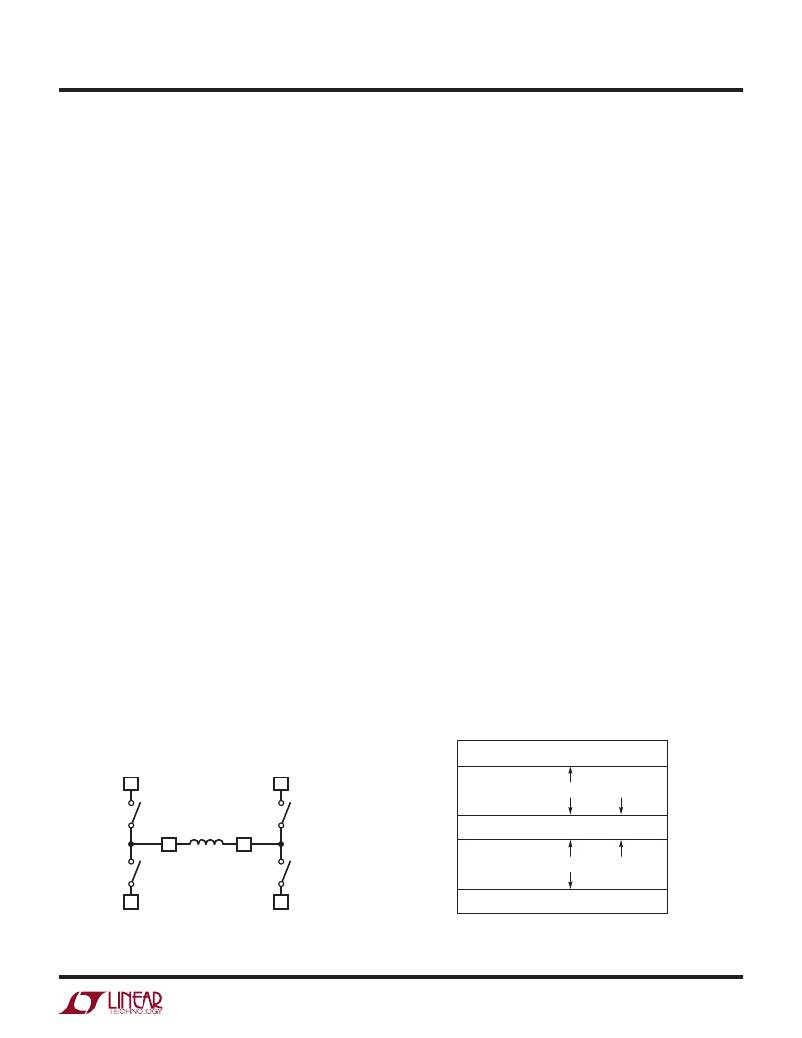
�Four-Switch� Control�
�Figure� 1� shows� a� simplified� diagram� of� how� the� four� internal�
�switches� are� connected� to� the� inductor,� PV� IN� ,� V� OUT� ,� PGND1�
�and� PGND2.� Figure� 2� shows� the� regions� of� operation� for�
�the� LTC3534� as� a� function� of� the� internal� control� voltage,�
�V� CI� .� Dependent� on� the� magnitude� of� V� CI� ,� the� LTC3534� will�
�operate� in� buck,� buck-boost� or� boost� mode.� V� CI� is� a� level�
�INTERNAL�
�DUTY� CONTROL�
�CYCLE� VOLTAGE,� V� CI�
�PV� IN�
�12�
�PMOS� A�
�SW1�
�5�
�L1�
�SW2�
�6�
�V� OUT�
�11�
�PMOS� D�
�85%�
�D� MAX�
�BOOST�
�D� MIN�
�BOOST�
�D� MAX�
�BUCK�
�A� ON,� B� OFF�
�PWM� C� AND� D�
�SWITCHES�
�FOUR� SWITCH� PWM�
�D� ON,� C� OFF�
�BOOST� REGION�
�BUCK-BOOST� REGION�
�V4� (� ~� 1.2V)�
�V3� (� ~� 720mV)�
�V2� (� ~� 640mV)�
�NMOS� B�
�4�
�PGND1�
�NMOS� C�
�7�
�3534� F01�
�PGND2�
�0%�
�PWM� A� AND� B�
�SWITCHES�
�BUCK� REGION�
�3534� F02�
�V1� (� ~� 100mV)�
�Figure� 1.� Simplified� Diagram� of� Output� Switches�
�Figure� 2.� Switch� Control� vs� Internal� Control� Voltage,� V� CI�
�3534fb�
�For� more� information� www.linear.com/LTC3534�
�9�
�相关PDF资料 |
PDF描述 |
|---|---|
| EL7212CS-T7 | IC DRIVER MOSFET DUAL HS 8-SOIC |
| ES1D-13 | RECT SUPER FAST SMD 200V 1A SMA |
| SDR1005-150ML | INDUCTOR PWR 15.0UH SMD |
| FPI | AC ADAPTER CLIP - INDIA |
| VE-B6J-CX-F1 | CONVERTER MOD DC/DC 36V 75W |
相关代理商/技术参数 |
参数描述 |
|---|---|
| DC1-2-28/12A | 制造商:未知厂家 制造商全称:未知厂家 功能描述:Analog IC |
| DC1-2-28/15A | 制造商:未知厂家 制造商全称:未知厂家 功能描述:Analog IC |
| DC1-2-28/24A | 制造商:未知厂家 制造商全称:未知厂家 功能描述:Analog IC |
| DC1-2-28/5A | 制造商:未知厂家 制造商全称:未知厂家 功能描述:Analog IC |
| DC1-2-28/9A | 制造商:未知厂家 制造商全称:未知厂家 功能描述:Analog IC |
发布紧急采购,3分钟左右您将得到回复。