- 您现在的位置:买卖IC网 > PDF目录19027 > DC1525A-E (Linear Technology)BOARD DEMO 40MSPS LTC2171-14 PDF资料下载
参数资料
| 型号: | DC1525A-E |
| 厂商: | Linear Technology |
| 文件页数: | 13/34页 |
| 文件大小: | 0K |
| 描述: | BOARD DEMO 40MSPS LTC2171-14 |
| 软件下载: | QuikEval II System |
| 设计资源: | DC1525A Design Files |
| 标准包装: | 1 |
| 系列: | * |
| 相关产品: | DC1371A-ND - BOARD USB DATA ACQUISITION HS |
第1页第2页第3页第4页第5页第6页第7页第8页第9页第10页第11页第12页当前第13页第14页第15页第16页第17页第18页第19页第20页第21页第22页第23页第24页第25页第26页第27页第28页第29页第30页第31页第32页第33页第34页
LTC2172-14/
LTC2171-14/LTC2170-14
20
21721014fb
CONVERTER OPERATION
TheLTC2172-14/LTC2171-14/LTC2170-14arelowpower,
4-channel, 14-bit, 65Msps/40Msps/25Msps A/D convert-
ers that are powered by a single 1.8V supply. The analog
inputs should be driven differentially. The encode input
can be driven differentially for optimal jitter performance,
or single-ended for lower power consumption. The digital
outputs are serial LVDS to minimize the number of data
lines. Each channel outputs two bits at a time (2-lane
mode) or one bit at a time (1-lane mode). Many additional
features can be chosen by programming the mode control
registers through a serial SPI port.
ANALOG INPUT
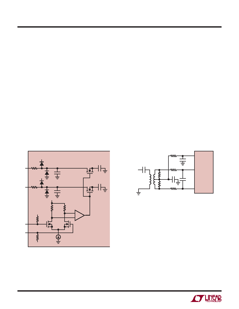
The analog inputs are differential CMOS sample-and-hold
circuits (Figure 2). The inputs should be driven differen-
tially around a common mode voltage set by the VCM12
applicaTions inForMaTion
or VCM34 output pins, which are nominally VDD/2. For the
2V input range, the inputs should swing from VCM – 0.5V
to VCM + 0.5V. There should be a 180° phase difference
between the inputs.
The four channels are simultaneously sampled by a
shared encode circuit (Figure 2).
INPUT DRIVE CIRCUITS
Input Filtering
If possible, there should be an RC lowpass filter right
at the analog inputs. This lowpass filter isolates the
drive circuitry from the A/D sample-and-hold switch-
ing and limits wideband noise from the drive circuitry.
Figure 3 shows an example of an input RC filter. The RC
component values should be chosen based on the ap-
plication’s input frequency.
Figure 2. Equivalent Input Circuit. Only One of
the Four Analog Channels Is Shown.
Figure 3. Analog Input Circuit Using a Transformer.
Recommended for Input Frequencies from 5MHz to 70MHz
CSAMPLE
3.5pF
RON
25
RON
25
VDD
LTC2172-14
AIN+
217214 F02
CSAMPLE
3.5pF
VDD
AIN–
ENC–
ENC+
1.2V
10k
1.2V
10k
CPARASITIC
1.8pF
CPARASITIC
1.8pF
10
25
50
0.1F
AIN+
AIN–
12pF
0.1F
VCM
LTC2172-14
ANALOG
INPUT
0.1F
T1
1:1
T1: MA/COM MABAES0060
RESISTORS, CAPACITORS
ARE 0402 PACKAGE SIZE
217214 F03
相关PDF资料 |
PDF描述 |
|---|---|
| SM3620S | LAMP T-1.5 TELE SLIDE 36V .02A |
| VX-5-1A2 | SWITCH BASIC SPDT 5A .187QC |
| SM2850S | LAMP T-1.5 TELE SLIDE 28V .05A |
| SM2450S | LAMP T-1.5 TELE SLIDE 24V .05A |
| SM1250S | LAMP T-1.5 TELE SLIDE 12V .05A |
相关代理商/技术参数 |
参数描述 |
|---|---|
| DC1525A-F | 功能描述:BOARD DEMO 25MSPS LTC2170-14 RoHS:是 类别:未定义的类别 >> 其它 系列:* 标准包装:1 系列:* 其它名称:MS305720A |
| DC1525A-G | 功能描述:BOARD DEMO 125MSPS LTC2175-12 RoHS:是 类别:未定义的类别 >> 其它 系列:* 标准包装:1 系列:* 其它名称:MS305720A |
| DC1525A-H | 功能描述:BOARD DEMO 105MSPS LTC2174-12 RoHS:是 类别:未定义的类别 >> 其它 系列:* 标准包装:1 系列:* 其它名称:MS305720A |
| DC1525A-I | 功能描述:BOARD DEMO 80MSPS LTC2173-12 RoHS:是 类别:未定义的类别 >> 其它 系列:* 标准包装:1 系列:* 其它名称:MS305720A |
| DC1525A-J | 功能描述:BOARD DEMO 65MSPS LTC2172-12 RoHS:是 类别:未定义的类别 >> 其它 系列:* 标准包装:1 系列:* 其它名称:MS305720A |
发布紧急采购,3分钟左右您将得到回复。