- 您现在的位置:买卖IC网 > PDF目录16613 > DC1561B (Linear Technology)EVAL BOARD FOR LTC4278 PDF资料下载
参数资料
| 型号: | DC1561B |
| 厂商: | Linear Technology |
| 文件页数: | 28/42页 |
| 文件大小: | 0K |
| 描述: | EVAL BOARD FOR LTC4278 |
| 标准包装: | 1 |
| 主要目的: | 电源管理,以太网供电(POE) |
| 嵌入式: | 否 |
| 已用 IC / 零件: | LTC4278 |
| 已供物品: | 板 |
第1页第2页第3页第4页第5页第6页第7页第8页第9页第10页第11页第12页第13页第14页第15页第16页第17页第18页第19页第20页第21页第22页第23页第24页第25页第26页第27页当前第28页第29页第30页第31页第32页第33页第34页第35页第36页第37页第38页第39页第40页第41页第42页
LTC4278
34
4278fc
design evaluates the switcher for short-circuit protection
and adds any additional circuitry to prevent destruction.
Output Voltage Error Sources
The LTC4278’s feedback sensing introduces additional
minor sources of errors. The following is a summary list:
Theinternalbandgapvoltagereferencesetsthereference
voltage for the feedback amplifier. The specifications
detail its variation.
The external feedback resistive divider ratio directly
affects regulated voltage. Use 1% components.
Leakage inductance on the transformer secondary
reduces the effective secondary-to-feedback winding
turns ratio (NS/NF) from its ideal value. This increases
the output voltage target by a similar percentage. Since
secondary leakage inductance is constant from part to
part (within a tolerance) adjust the feedback resistor
ratio to compensate.
The transformer secondary current flows through the
impedances of the winding resistance, synchronous
MOSFET RDS(ON) and output capacitor ESR. The DC
equivalent current for these errors is higher than the
load current because conduction occurs only during
the converter’s off-time. So, divide the load current by
(1 – DC).
Iftheoutputloadcurrentisrelativelyconstant,thefeedback
resistive divider is used to compensate for these losses.
Otherwise, use the LTC4278 load compensation circuitry
(see Load Compensation). If multiple output windings are
used, the flyback winding will have a signal that represents
an amalgamation of all these windings impedances. Take
carethatyouexamineworst-caseloadingconditionswhen
tweaking the voltages.
Power MOSFET Selection
ThepowerMOSFETsareselectedprimarilyonthecriteriaof
on-resistance RDS(ON),inputcapacitance,drain-to-source
breakdown voltage (BVDSS), maximum gate voltage (VGS)
and maximum drain current (ID(MAX)).
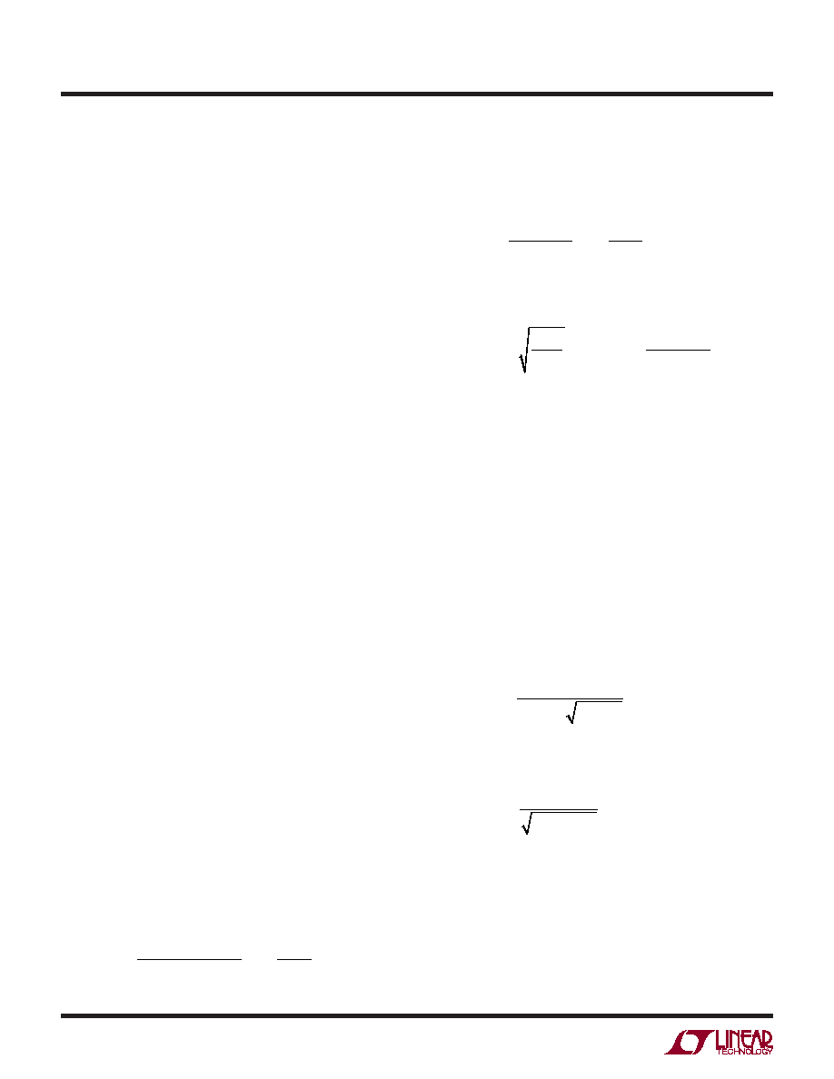
For the primary-side power MOSFET, the peak current is:
IPK(PRI) =
PIN
VIN(MIN) DCMAX
1+ XMIN
2
APPLICATIONS INFORMATION
where XMINispeak-to-peakcurrentratioasdefinedearlier.
For each secondary-side power MOSFET, the peak cur-
rent is:
IPK(SEC) =
IOUT
1DCMAX
1+ XMIN
2
Select a primary-side power MOSFET with a BVDSS
greater than:
BVDSS ≥IPK
LLKG
CP
+ VIN(MAX) +
VOUT(MAX)
NSP
where NSP reflects the turns ratio of that secondary-to
primary winding. LLKG is the primary-side leakage induc-
tanceandCPistheprimary-sidecapacitance(mostlyfrom
the drain capacitance (COSS) of the primary-side power
MOSFET). A clamp may be added to reduce the leakage
inductance as discussed.
Foreachsecondary-sidepowerMOSFET,theBVDSSshould
be greater than:
BVDSS ≥ VOUT + VIN(MAX) NSP
Choose the primary-side MOSFET RDS(ON) at the nominal
gatedrivevoltage(7.5V).Thesecondary-sideMOSFETgate
drive voltage depends on the gate drive method.
Primary-side power MOSFET RMS current is given by:
IRMS(PRI) =
PIN
VIN(MIN) DCMAX
For each secondary-side power MOSFET RMS current is
given by:
IRMS(SEC) =
IOUT
1– DCMAX
Calculate MOSFET power dissipation next. Because the
primary-side power MOSFET operates at high VDS, a
transitionpowerlosstermisincludedforaccuracy.CMILLER
is the most critical parameter in determining the transition
loss, but is not directly specified on the data sheets.
相关PDF资料 |
PDF描述 |
|---|---|
| H3BKH-2006M | IDC CABLE - HSR20H/AE20M/HPK20H |
| RBM18DCTD-S288 | CONN EDGECARD 36POS .156 EXTEND |
| REC5-4815DRW/H6/A | CONV DC/DC 5W 36-72VIN +/-15VOUT |
| V110C24C100B | CONVERTER MOD DC/DC 24V 100W |
| RSA06DRST-S288 | CONN EDGECARD 12POS .125 EXTEND |
相关代理商/技术参数 |
参数描述 |
|---|---|
| DC1561W | 制造商:Aleph America Corporation 功能描述: |
| DC1561W-COM | 制造商:Aleph America Corporation 功能描述: |
| DC1562A-A | 功能描述:BOARD EVAL LTC6990 RoHS:是 类别:编程器,开发系统 >> 评估演示板和套件 系列:TimerBlox® 标准包装:1 系列:- 主要目的:电信,线路接口单元(LIU) 嵌入式:- 已用 IC / 零件:IDT82V2081 主要属性:T1/J1/E1 LIU 次要属性:- 已供物品:板,电源,线缆,CD 其它名称:82EBV2081 |
| DC1562A-B | 功能描述:BOARD EVAL LTC6991 RoHS:是 类别:编程器,开发系统 >> 评估演示板和套件 系列:TimerBlox® 标准包装:1 系列:- 主要目的:电信,线路接口单元(LIU) 嵌入式:- 已用 IC / 零件:IDT82V2081 主要属性:T1/J1/E1 LIU 次要属性:- 已供物品:板,电源,线缆,CD 其它名称:82EBV2081 |
| DC1562A-C | 功能描述:BOARD EVAL LTC6992-1 RoHS:是 类别:编程器,开发系统 >> 评估演示板和套件 系列:TimerBlox® 标准包装:1 系列:- 主要目的:数字电位器 嵌入式:- 已用 IC / 零件:AD5258 主要属性:- 次要属性:- 已供物品:板 相关产品:AD5258BRMZ1-ND - IC POT DGTL I2C1K 64P 10MSOPAD5258BRMZ10-ND - IC POT DGTL I2C 10K 64P 10MSOPAD5258BRMZ100-ND - IC POT DGTL I2C 100K 64P 10MSOPAD5258BRMZ50-ND - IC POT DGTL I2C 50K 64P 10MSOPAD5258BRMZ1-R7-ND - IC POT DGTL I2C 1K 64P 10MSOPAD5258BRMZ10-R7-ND - IC POT DGTL I2C 10K 64P 10MSOPAD5258BRMZ50-R7-ND - IC POT DGTL I2C 50K 64P 10MSOPAD5258BRMZ100-R7-ND - IC POT DGTL I2C 100K 64P 10MSOP |
发布紧急采购,3分钟左右您将得到回复。