- 您现在的位置:买卖IC网 > PDF目录16542 > DC1562A-J (Linear Technology)BOARD EVAL LTC6993-4 PDF资料下载
参数资料
| 型号: | DC1562A-J |
| 厂商: | Linear Technology |
| 文件页数: | 13/26页 |
| 文件大小: | 0K |
| 描述: | BOARD EVAL LTC6993-4 |
| 设计资源: | DC1562A Design Files DC1562A Schematic |
| 特色产品: | TimerBlox? |
| 标准包装: | 1 |
| 系列: | TimerBlox® |
| 主要目的: | 定时,单稳多谐振荡器 |
| 嵌入式: | 否 |
| 已用 IC / 零件: | LTC6993-4 |
| 主要属性: | 下降沿触发器,可再触发 |
| 次要属性: | 2.25 V ~ 5.5 V 电源 |
| 已供物品: | 板 |
LTC6993-1/LTC6993-2
LTC6993-3/LTC6993-4
20
69931234fb
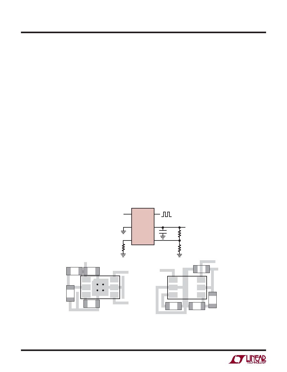
Supply Bypassing and PCB Layout Guidelines
TheLTC6993isanaccuratemonostablemultivibratorwhen
used in the appropriate manner. The part is simple to use
and by following a few rules, the expected performance is
easily achieved. Adequate supply bypassing and proper
PCB layout are important to ensure this.
Figure 13 shows example PCB layouts for both the SOT-23
and DCB packages using 0603 sized passive components.
The layouts assume a two layer board with a ground plane
layer beneath and around the LTC6993. These layouts are
a guide and need not be followed exactly.
1. Connect the bypass capacitor, C1, directly to the V+ and
GND pins using a low inductance path. The connection
from C1 to the V+ pin is easily done directly on the top
layer. For the DCB package, C1’s connection to GND is
also simply done on the top layer. For the SOT-23, OUT
can be routed through the C1 pads to allow a good C1
GND connection. If the PCB design rules do not allow
that,C1’sGNDconnectioncanbeaccomplishedthrough
multiple vias to the ground plane. Multiple vias for both
the GND pin connection to the ground plane and the
C1 connection to the ground plane are recommended
to minimize the inductance. Capacitor C1 should be a
0.1F ceramic capacitor.
2. Place all passive components on the top side of the
board. This minimizes trace inductance.
3. Place RSET as close as possible to the SET pin and
make a direct, short connection. The SET pin is a cur-
rent summing node and currents injected into this pin
directlymodulatetheoutputpulsewidth.Havingashort
connection minimizes the exposure to signal pickup.
4. Connect RSET directly to the GND pin. Using a long path
or vias to the ground plane will not have a significant
affect on accuracy, but a direct, short connection is
recommended and easy to apply.
5. Use a ground trace to shield the SET pin. This provides
another layer of protection from radiated signals.
6. Place R1 and R2 close to the DIV pin. A direct, short
connection to the DIV pin minimizes the external signal
coupling.
69931234 F13
LTC6993
TRIG
GND
SET
OUT
V+
DIV
C1
0.1F
R1
R2
RSET
V+
DIV
SET
OUT
GND
TRIG
C1
R1
R2
V+
RSET
DCB PACKAGE
TRIG
GND
SET
OUT
V+
DIV
R2
V+
RSET
TSOT-23 PACKAGE
R1
C1
Figure 13. Supply Bypassing and PCB Layout
APPLICATIONS INFORMATION
相关PDF资料 |
PDF描述 |
|---|---|
| H3DWH-4018G | IDC CABLE - HKR40H/AE40G/HPL40H |
| MEC1-120-02-F-D-EM2 | CONN EDGE CARD DL 40POS SMD |
| ILC0603ERR15K | INDUCTOR CER 150NH 0603 |
| RBC08DRYS-S734 | CONN EDGECARD 16POS DIP .100 SLD |
| ECM31DCTD-S288 | CONN EDGECARD 62POS .156 EXTEND |
相关代理商/技术参数 |
参数描述 |
|---|---|
| DC1562A-K | 功能描述:BOARD EVAL LTC6994-1 RoHS:是 类别:编程器,开发系统 >> 评估演示板和套件 系列:TimerBlox® 标准包装:1 系列:- 主要目的:电信,线路接口单元(LIU) 嵌入式:- 已用 IC / 零件:IDT82V2081 主要属性:T1/J1/E1 LIU 次要属性:- 已供物品:板,电源,线缆,CD 其它名称:82EBV2081 |
| DC1562A-L | 功能描述:BOARD EVAL LTC6994-2 RoHS:是 类别:编程器,开发系统 >> 评估演示板和套件 系列:TimerBlox® 标准包装:1 系列:- 主要目的:电信,线路接口单元(LIU) 嵌入式:- 已用 IC / 零件:IDT82V2081 主要属性:T1/J1/E1 LIU 次要属性:- 已供物品:板,电源,线缆,CD 其它名称:82EBV2081 |
| DC1562B-B | 制造商:Linear Technology 功能描述:LTC6991 DEMO BOARD 1Hz (1s) Fixed Frequenc |
| DC1562B-C | 制造商:Linear Technology 功能描述:LTC6992-1 DEMO BOARD 10kHz, 0 100% Duty Cycle |
| DC1562B-E | 制造商:Linear Technology 功能描述:BOARD EVAL LTC6992-3 制造商:Linear Technology 功能描述:DEMO BOARD LTC6992-3 VOLTAGE CONTROLLED 制造商:Linear Technology 功能描述:DEMO BOARD, LTC6992-3 VOLTAGE CONTROLLED 制造商:Linear Technology 功能描述:DEMO BOARD, LTC6992-3 VOLTAGE CONTROLLED OSC, Silicon Manufacturer:Linear Technology, Silicon Core Number:LTC6992-3, Kit Application Type:Clock & Timing, Application Sub Type:Voltage Controlled Oscillator |
发布紧急采购,3分钟左右您将得到回复。