- 您现在的位置:买卖IC网 > PDF目录17065 > DC586A (Linear Technology)BOARD DELTA SIGMA ADC LTC2431 PDF资料下载
参数资料
| 型号: | DC586A |
| 厂商: | Linear Technology |
| 文件页数: | 17/40页 |
| 文件大小: | 0K |
| 描述: | BOARD DELTA SIGMA ADC LTC2431 |
| 软件下载: | QuikEval System |
| 设计资源: | DC586A Design File DC586A Schematic |
| 标准包装: | 1 |
| 系列: | QuikEval™ |
| ADC 的数量: | 2 |
| 位数: | 20 |
| 采样率(每秒): | 7.5 |
| 数据接口: | MICROWIRE?,串行,SPI? |
| 工作温度: | 0°C ~ 70°C |
| 已用 IC / 零件: | LTC2431 |
| 已供物品: | 板 |
| 相关产品: | DC590B-ND - BOARD DEMO USB SERIAL CONTROLLER LTC2431IMS#PBF-ND - IC ADC 20BIT DIFFINPUT/REF10MSOP LTC2431CMS#TRPBF-ND - IC ADC 20BIT DIFFINPUT/REF10MSOP LTC2431IMS#TRPBF-ND - IC ADC 20BIT DIFFINPUT/REF10MSOP LTC2431CMS#PBF-ND - IC ADC 20BIT DIFFINPUT/REF10MSOP LTC2431CMS-ND - IC ADC 20BIT DIFFINPUT/REF10MSOP LTC2431IMSTR-ND - IC ADC 20BIT DIFFINPUT/REF10MSOP LTC2431IMS-ND - IC ADC 20BIT DIFFINPUT/REF10MSOP LTC2431CMSTR-ND - IC ADC 20BIT DIFFINPUT/REF10MSOP |
第1页第2页第3页第4页第5页第6页第7页第8页第9页第10页第11页第12页第13页第14页第15页第16页当前第17页第18页第19页第20页第21页第22页第23页第24页第25页第26页第27页第28页第29页第30页第31页第32页第33页第34页第35页第36页第37页第38页第39页第40页
LTC2430/LTC2431
24
24301f
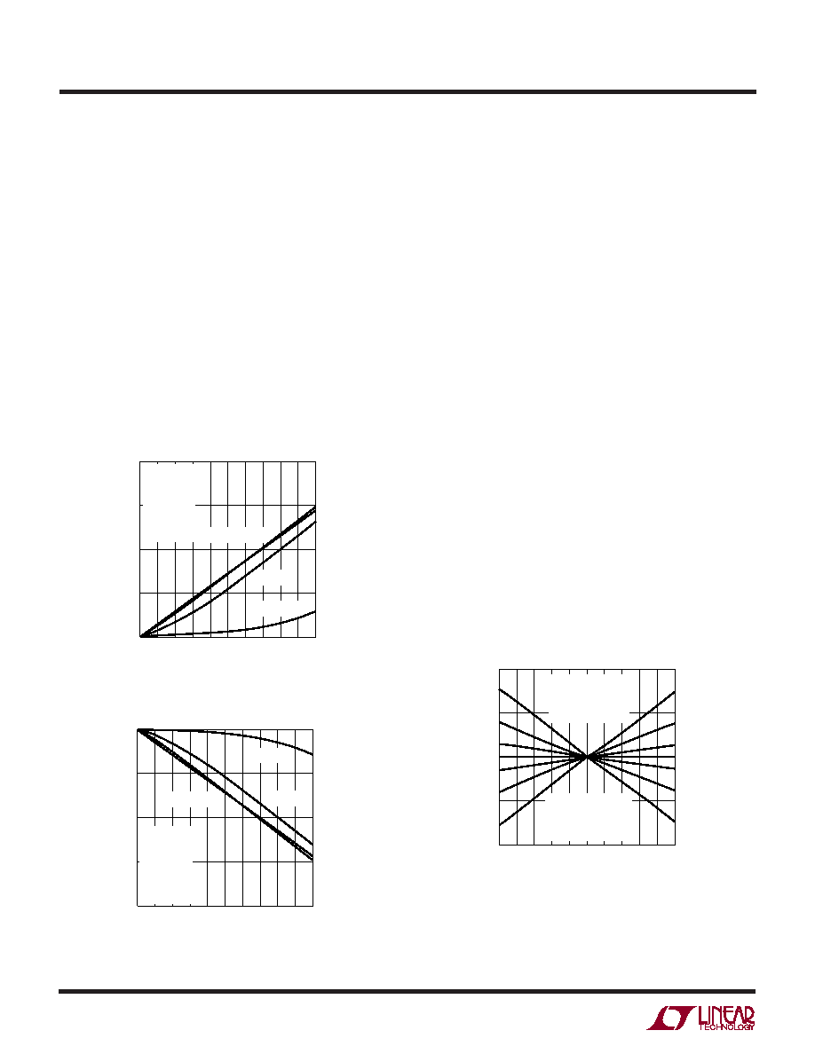
The typical +FS and –FS errors as a function of the sum of
the source resistance seen by IN+ and IN– for large values
of CIN are shown in Figure 15.
In addition to this gain error, an offset error term may also
appear. The offset error is proportional with the mismatch
between the source impedance driving the two input pins
IN+ and IN– and with the difference between the input and
reference common mode voltages. While the input drive
circuit nonzero source impedance combined with the
converter average input current will not degrade the INL
performance, indirect distortion may result from the modu-
lation of the offset error by the common mode component
of the input signal. Thus, when using large CIN capacitor
values, it is advisable to carefully match the source imped-
ance seen by the IN+ and IN– pins. When FO = LOW
(internal oscillator and 60Hz notch), every 1
mismatch
in source impedance transforms a full-scale common
mode input signal into a differential mode input signal of
0.023ppm. When FO = HIGH (internal oscillator and 50Hz
notch), every 1
mismatch in source impedance trans-
forms a full-scale common mode input signal into a
differential mode input signal of 0.019ppm. When FO is
driven by an external oscillator with a frequency fEOSC,
every 1
mismatch in source impedance transforms a
full-scale common mode input signal into a differential
mode input signal of 0.15 10–6 fEOSCppm. Figure 16
shows the typical offset error due to input common mode
voltage for various values of source resistance imbalance
between the IN+ and IN– pins when large CIN values are
used.
If possible, it is desirable to operate with the input signal
common mode voltage very close to the reference signal
common mode voltage as is the case in the ratiometric
measurement of a symmetric bridge. This configuration
eliminates the offset error caused by mismatched source
impedances.
The magnitude of the dynamic input current depends upon
the size of the very stable internal sampling capacitors and
upon the accuracy of the converter sampling clock. The
accuracy of the internal clock over the entire temperature
and power supply range is typically better than 1%. Such
APPLICATIO S I FOR ATIO
WU
UU
Figure 15a. + FS Error vs RSOURCE at IN+ or IN– (Large CIN)
Figure 15b. – FS Error vs RSOURCE at IN
+ or IN– (Large CIN)
RSOURCE ()
0
+FS
ERROR
(ppm)
10
15
800
2431 F15a
5
0
200
400 500
1000
20
600
100
300
900
700
CIN = 0.01F
CIN = 0.1F
CIN = 1F, 10F
VCC = 5V
VREF+ = 5V
VREF– = GND
VIN+ = 3.75V
VIN– = 1.25V
FO = GND
TA = 25°C
RSOURCE ()
0
–
FS
ERROR
(ppm)
–10
–5
800
2431 F15b
–15
–20
200
400 500
1000
0
600
100
300
900
700
CIN = 0.01F
CIN = 0.1F
CIN = 1F, 10F
VCC = 5V
VREF+ = 5V
VREF– = GND
VIN+ = 1.25V
VIN– = 3.75V
FO = GND
TA = 25°C
Figure 16. Offset Error vs Common Mode Voltage
(VINCM = VIN+ = VIN–) and Input Source Resistance Imbalance
(
RIN = RSOURCEIN+ – RSOURCEIN–) for Large CIN Values (CIN ≥ 1F)
VINCM (V)
0
OFFSET
ERROR
(ppm)
0
20
4
–20
–40
1
2
2.5
5
40
A
B
C
D
E
F
G
3
0.5
1.5
4.5
3.5
VCC = 5V
VREF+ = 5V
VREF– = GND
VIN+ = VIN– = VINCM
FO = GND
RSOURCEIN– = 500
CIN = 10F
TA = 25°C
2431 F16
A:
RIN = +1k
B:
RIN = +500
C:
RIN = +200
D:
RIN = 0
E:
RIN = –200
F:
RIN = –500
G:
RIN = –1k
相关PDF资料 |
PDF描述 |
|---|---|
| 0210490987 | CABLE JUMPER 1.25MM .030M 29POS |
| AP2192SG-13 | IC PWR SW USB 2CH 1.5A 8-SOIC |
| 381LX470M450H022 | CAP ALUM 47UF 450V 20% SNAP |
| DC847A | BOARD DELTA SIGMA ADC LTC2446 |
| DC790A | BOARD DELTA SIGMA ADC LTC2439-1 |
相关代理商/技术参数 |
参数描述 |
|---|---|
| DC-58F BLACK | 制造商:Polycase 功能描述:Enclosure, Flanged, Flame Retardant ABS Plastic, 8.25 x 5.0 x 3.0 in, Black |
| DC-58F LIGHT GRAY | 制造商:Polycase 功能描述:Enclosure, Flanged, Flame Retardant ABS Plastic, 8.25 x 5.00 x 3.00 in, Gray |
| DC-58FMBYT | 制造商:Polycase 功能描述:Enclosure, Flanged, Panel Mount, ABS,UL94-5VA, Black, 8.25x5x3 In, DC Series |
| DC-58FMBYT01 | 制造商:Polycase 功能描述:Enclosure;Flanged;PanelMount;ABS,UL94-5VA;Gray;8.25x5x3 In;DC Series |
| DC-58PMBYT | 制造商:Polycase 功能描述:Enclosure;Box-Lid;Desktop;ABS,UL94-5VA;Black;8.25x5x3 In;DC Series |
发布紧急采购,3分钟左右您将得到回复。