- 您现在的位置:买卖IC网 > PDF目录17065 > DC586A (Linear Technology)BOARD DELTA SIGMA ADC LTC2431 PDF资料下载
参数资料
| 型号: | DC586A |
| 厂商: | Linear Technology |
| 文件页数: | 6/40页 |
| 文件大小: | 0K |
| 描述: | BOARD DELTA SIGMA ADC LTC2431 |
| 软件下载: | QuikEval System |
| 设计资源: | DC586A Design File DC586A Schematic |
| 标准包装: | 1 |
| 系列: | QuikEval™ |
| ADC 的数量: | 2 |
| 位数: | 20 |
| 采样率(每秒): | 7.5 |
| 数据接口: | MICROWIRE?,串行,SPI? |
| 工作温度: | 0°C ~ 70°C |
| 已用 IC / 零件: | LTC2431 |
| 已供物品: | 板 |
| 相关产品: | DC590B-ND - BOARD DEMO USB SERIAL CONTROLLER LTC2431IMS#PBF-ND - IC ADC 20BIT DIFFINPUT/REF10MSOP LTC2431CMS#TRPBF-ND - IC ADC 20BIT DIFFINPUT/REF10MSOP LTC2431IMS#TRPBF-ND - IC ADC 20BIT DIFFINPUT/REF10MSOP LTC2431CMS#PBF-ND - IC ADC 20BIT DIFFINPUT/REF10MSOP LTC2431CMS-ND - IC ADC 20BIT DIFFINPUT/REF10MSOP LTC2431IMSTR-ND - IC ADC 20BIT DIFFINPUT/REF10MSOP LTC2431IMS-ND - IC ADC 20BIT DIFFINPUT/REF10MSOP LTC2431CMSTR-ND - IC ADC 20BIT DIFFINPUT/REF10MSOP |
第1页第2页第3页第4页第5页当前第6页第7页第8页第9页第10页第11页第12页第13页第14页第15页第16页第17页第18页第19页第20页第21页第22页第23页第24页第25页第26页第27页第28页第29页第30页第31页第32页第33页第34页第35页第36页第37页第38页第39页第40页
LTC2430/LTC2431
14
24301f
+FS, the conversion result is clamped to the value corre-
sponding to the +FS + 1LSB. For differential input voltages
below –FS, the conversion result is clamped to the value
corresponding to –FS – 1LSB.
Frequency Rejection Selection (FO)
The LTC2430/LTC2431 internal oscillator provides better
than 110dB normal mode rejection at the line frequency
and all its harmonics for 50Hz
±2% or 60Hz ±2%. For
60Hz rejection, FO should be connected to GND while for
50Hz rejection the FO pin should be connected to VCC.
The selection of 50Hz or 60Hz rejection can also be made
by driving FO to an appropriate logic level. A selection
change during the sleep or data output states will not
disturb the converter operation. If the selection is made
during the conversion state, the result of the conversion in
progress may be outside specifications but the following
conversions will not be affected.
When a fundamental rejection frequency different from
50Hz or 60Hz is required or when the converter must be
synchronized with an outside source, the LTC2430 or
LTC2431 can operate with an external conversion clock.
The converter automatically detects the presence of an
external clock signal at the FO pin and turns off the internal
oscillator. The frequency fEOSC of the external signal must
be at least 5kHz to be detected. The external clock signal
duty cycle is not significant as long as the minimum and
maximum specifications for the high and low periods tHEO
and tLEO are observed.
While operating with an external conversion clock of a
frequency fEOSC, the LTC2430 or LTC2431 provides better
than 110dB normal mode rejection in a frequency range
fEOSC/2560 ±4% and its harmonics. The normal mode
rejection as a function of the input frequency deviation
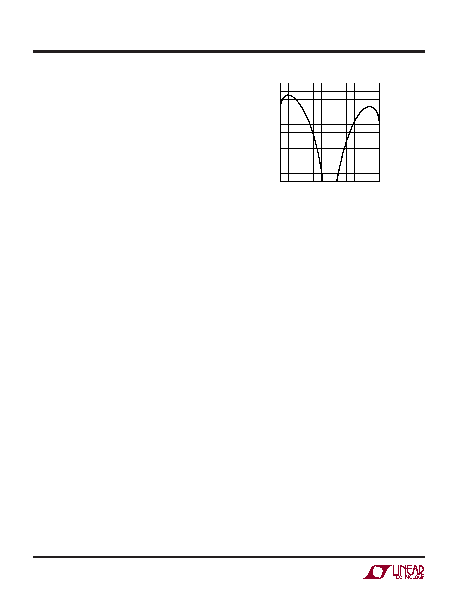
from fEOSC/2560 is shown in Figure 4.
Whenever an external clock is not present at the FO pin, the
converter (LTC2430 or LTC2431) automatically activates
its internal oscillator and enters the Internal Conversion
Clock mode. Its operation will not be disturbed if the
change of conversion clock source occurs during the
sleep state or during the data output state while the con-
verter uses an external serial clock. If the change occurs
during the conversion state, the result of the conversion in
progress may be outside specifications but the following
conversions will not be affected. If the change occurs
during the data output state and the converter is in the
Internal SCK mode, the serial clock duty cycle may be
affected but the serial data stream will remain valid.
Table 3 summarizes the duration of each state and the
achievable output data rate as a function of FO.
SERIAL INTERFACE PINS
The LTC2430/LTC2431 transmit the conversion results
and receives the start of conversion command through a
synchronous 3-wire interface. During the conversion and
sleep states, this interface can be used to assess the
converter status and during the data output state it is used
to read the conversion result.
Serial Clock Input/Output (SCK)
The serial clock signal present on SCK is used to synchro-
nize the data transfer. Each bit of data is shifted out the
SDO pin on the falling edge of the serial clock.
In the Internal SCK mode of operation, the SCK pin is an
output and the converter (LTC2430 or LTC2431) creates
its own serial clock by dividing the internal conversion clock
by 8. In the External SCK mode of operation, the SCK pin
is used as input. The internal or external SCK mode is
selected on power-up and then reselected every time a
HIGH-to-LOW transition is detected at the CS pin. If SCK
Figure 4. LTC2430/LTC2431 Normal Mode Rejection When
Using an External Oscillator of Frequency fEOSC
APPLICATIO S I FOR ATIO
WU
UU
DIFFERENTIAL INPUT SIGNAL FREQUENCY
DEVIATION FROM NOTCH FREQUENCY fEOSC/2560(%)
–12
–8
–4
048
12
NORMAL
MODE
REJECTION
(dB)
2431 F04
–80
–85
–90
–95
–100
–105
–110
–115
–120
–125
–130
–135
–140
相关PDF资料 |
PDF描述 |
|---|---|
| 0210490987 | CABLE JUMPER 1.25MM .030M 29POS |
| AP2192SG-13 | IC PWR SW USB 2CH 1.5A 8-SOIC |
| 381LX470M450H022 | CAP ALUM 47UF 450V 20% SNAP |
| DC847A | BOARD DELTA SIGMA ADC LTC2446 |
| DC790A | BOARD DELTA SIGMA ADC LTC2439-1 |
相关代理商/技术参数 |
参数描述 |
|---|---|
| DC-58F BLACK | 制造商:Polycase 功能描述:Enclosure, Flanged, Flame Retardant ABS Plastic, 8.25 x 5.0 x 3.0 in, Black |
| DC-58F LIGHT GRAY | 制造商:Polycase 功能描述:Enclosure, Flanged, Flame Retardant ABS Plastic, 8.25 x 5.00 x 3.00 in, Gray |
| DC-58FMBYT | 制造商:Polycase 功能描述:Enclosure, Flanged, Panel Mount, ABS,UL94-5VA, Black, 8.25x5x3 In, DC Series |
| DC-58FMBYT01 | 制造商:Polycase 功能描述:Enclosure;Flanged;PanelMount;ABS,UL94-5VA;Gray;8.25x5x3 In;DC Series |
| DC-58PMBYT | 制造商:Polycase 功能描述:Enclosure;Box-Lid;Desktop;ABS,UL94-5VA;Black;8.25x5x3 In;DC Series |
发布紧急采购,3分钟左右您将得到回复。