- 您现在的位置:买卖IC网 > PDF目录17063 > DC845A (Linear Technology)BOARD DELTA SIGMA ADC LTC2448 PDF资料下载
参数资料
| 型号: | DC845A |
| 厂商: | Linear Technology |
| 文件页数: | 14/28页 |
| 文件大小: | 0K |
| 描述: | BOARD DELTA SIGMA ADC LTC2448 |
| 软件下载: | QuikEval System |
| 设计资源: | DC845A Design File DC845A Schematic |
| 标准包装: | 1 |
| 系列: | QuikEval™ |
| ADC 的数量: | 1 |
| 位数: | 24 |
| 采样率(每秒): | 8k |
| 数据接口: | MICROWIRE?,串行,SPI? |
| 已用 IC / 零件: | LTC2448 |
| 已供物品: | 板 |
| 相关产品: | LTC2448IUHF#PBF-ND - IC ADC 24BIT HI SPEED 38QFN LTC2448CUHF#PBF-ND - IC ADC 24BIT HI SPEED 38QFN LTC2448IUHF#TRPBF-ND - IC ADC 24BIT HI SPEED 38QFN LTC2448CUHF#TRPBF-ND - IC ADC 24BIT HI SPEED 38QFN LTC2448CUHF-ND - IC ADC 24BIT HI SPEED 38QFN LTC2448IUHF-ND - IC ADC 24BIT HI SPEED 38QFN LTC2448CUHF#TR-ND - IC ADC 24BIT HI SPEED 38QFN LTC2448IUHF#TR-ND - IC ADC 24BIT HI SPEED 38QFN |
第1页第2页第3页第4页第5页第6页第7页第8页第9页第10页第11页第12页第13页当前第14页第15页第16页第17页第18页第19页第20页第21页第22页第23页第24页第25页第26页第27页第28页
LTC2444/LTC2445/
LTC2448/LTC2449
21
2444589fb
APPLICATIO S I FOR ATIO
WU
U
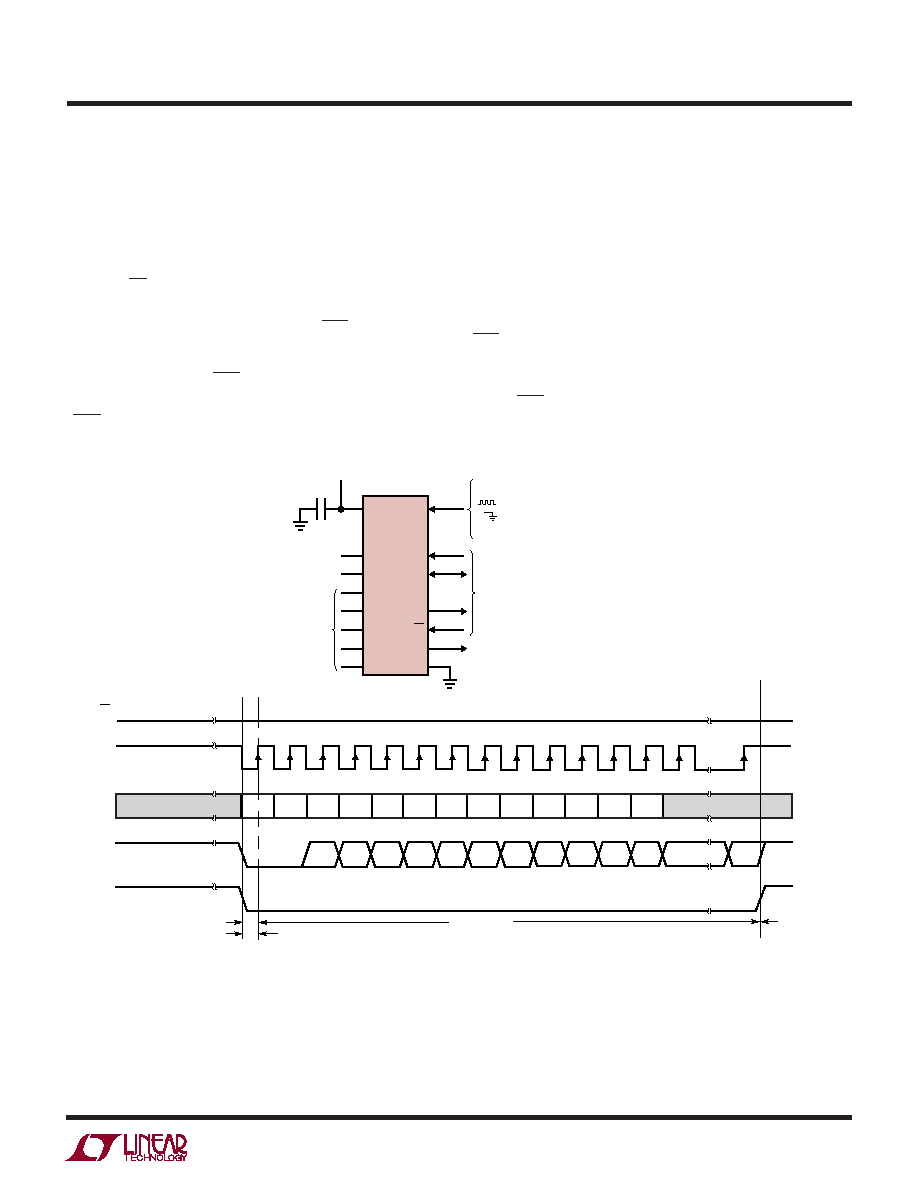
Figure 9. Internal Serial Clock, Continuous Operation
CS
SCK
SDI
SDO
BUSY
2444 F10
CONVERSION
SLEEP
DATA OUTPUT
CONVERSION
MSB
BIT 28 BIT 27 BIT 26 BIT 25 BIT 24 BIT 23 BIT 22 BIT 21
BIT 20 BIT 19
BIT 0
LSB
SIG
BIT 29
“0”
BIT 30
EOC
BIT 31
1
0
EN
SGL
A2
A1
A0
OSR3
OSR2
OSR1
OSR0
TWOX
ODD
12345
6
7
89
10
11
12
13
14
32
DON'T CARE
VCC
FO
REF+
REF–
CH0
CH7
CH8
CH15
COM
SCK
SDI
SDO
CS
GND
28
35
29
30
8
15
16
23
7
38
37
1,4,5,6,31,32,33,39
36
34
REFERENCE
VOLTAGE
0.1V TO VCC
ANALOG
INPUTS
2
= EXTERNAL OSCILLATOR
= INTERNAL OSCILLATOR
1
F
4.5V TO 5.5V
LTC2448
4-WIRE
SPI INTERFACE
BUSY
Internal Serial Clock, 2-Wire I/O,
Continuous Conversion
This timing mode uses a 2-wire, all output (SCK and SDO)
interface. The conversion result is shifted out of the device
by an internally generated serial clock (SCK) signal, see
Figure 9. CS may be permanently tied to ground, simplify-
ing the user interface or isolation barrier. The internal
serial clock mode is selected by tying EXT HIGH.
During the conversion, the SCK and the serial data output
pin (SDO) are HIGH (EOC = 1) and BUSY = 1. Once the
conversion is complete, SCK, BUSY and SDO go LOW
(EOC = 0) indicating the conversion has finished and the
device has entered the low power sleep state. The part
remains in the sleep state a minimum amount of time
(
≈500ns) then immediately begins outputting data. The
data output cycle begins on the first rising edge of SCK and
ends after the 32nd rising edge. Data is shifted out the SDO
pin on each falling edge of SCK. The internally generated
serial clock is output to the SCK pin. This signal may be
used to shift the conversion result into external circuitry.
EOC can be latched on the first rising edge of SCK and the
last bit of the conversion result can be latched on the 32nd
rising edge of SCK. After the 32nd rising edge, SDO goes
HIGH (EOC = 1) indicating a new conversion is in progress.
SCK remains HIGH during the conversion.
相关PDF资料 |
PDF描述 |
|---|---|
| 0210490277 | CABLE JUMPER 1.25MM .030M 22POS |
| RBM08DCBS-S189 | CONN EDGECARD 16POS R/A .156 SLD |
| 0210391080 | CABLE JUMPER 1MM .102M 37POS |
| DC682A | BOARD SAR ADC LTC1859 |
| EBM12DTBT-S189 | CONN EDGECARD 24POS R/A .156 SLD |
相关代理商/技术参数 |
参数描述 |
|---|---|
| DC846A | 功能描述:BOARD DELTA SIGMA ADC LTC2447 RoHS:是 类别:编程器,开发系统 >> 评估板 - 模数转换器 (ADC) 系列:QuikEval™ 产品培训模块:Obsolescence Mitigation Program 标准包装:1 系列:- ADC 的数量:1 位数:12 采样率(每秒):94.4k 数据接口:USB 输入范围:±VREF/2 在以下条件下的电源(标准):- 工作温度:-40°C ~ 85°C 已用 IC / 零件:MAX11645 已供物品:板,软件 |
| DC847A | 功能描述:BOARD DELTA SIGMA ADC LTC2446 RoHS:是 类别:编程器,开发系统 >> 评估板 - 模数转换器 (ADC) 系列:QuikEval™ 产品培训模块:Obsolescence Mitigation Program 标准包装:1 系列:- ADC 的数量:1 位数:12 采样率(每秒):94.4k 数据接口:USB 输入范围:±VREF/2 在以下条件下的电源(标准):- 工作温度:-40°C ~ 85°C 已用 IC / 零件:MAX11645 已供物品:板,软件 |
| DC850 | 制造商:Molex 功能描述: |
| DC852A | 功能描述:BOARD DEMO FOR LTC4354 RoHS:是 类别:未定义的类别 >> 其它 系列:* 标准包装:1 系列:* 其它名称:MS305720A |
| DC8550 | 制造商:DCCOM 制造商全称:Dc Components 功能描述:TECHNICAL SPECIFICATIONS OF PNP EPITAXIAL PLANAR TRANSISTOR |
发布紧急采购,3分钟左右您将得到回复。