- 您现在的位置:买卖IC网 > PDF目录258144 > DG190AP (VISHAY SILICONIX) DUAL 1-CHANNEL, SGL POLE DOUBLE THROW SWITCH, DIP16 PDF资料下载
参数资料
| 型号: | DG190AP |
| 厂商: | VISHAY SILICONIX |
| 元件分类: | 多路复用及模拟开关 |
| 英文描述: | DUAL 1-CHANNEL, SGL POLE DOUBLE THROW SWITCH, DIP16 |
| 封装: | SIDE BRAZED, DIP-16 |
| 文件页数: | 1/9页 |
| 文件大小: | 109K |
| 代理商: | DG190AP |
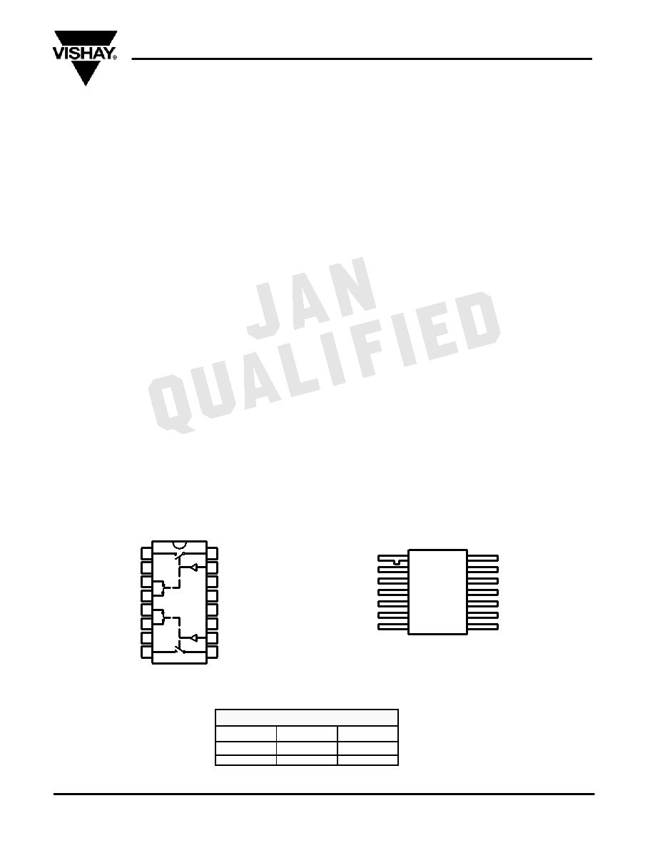
*Common to Substrate and Case
Flat Package
S4
S3
D4
D3
D2
D1
S2
S1
IN2
IN1
V+
V*
VL
VR
1
2
3
4
5
6
7
14
13
12
11
10
9
8
Top View
D1
S1
NC
Dual-In-Line
IN1
D3
V
S3
VR
S4
VL
D4
V+
NC
IN2
D2
S2
1
2
3
4
5
6
7
8
16
15
14
13
12
11
10
9
Top View
Refer to JAN38510 Information, Military Section
DG189/190/191
Vishay Siliconix
Document Number: 70034
S-51140—Rev. D, 20-Jun-05
www.vishay.com
1
High-Speed Drivers with Dual SPDT JFET Switches
FEATURES
BENEFITS
APPLICATIONS
D Constant On-Resistance Over
Entire Analog Range
D Low Leakage
D Low Crosstalk
D Rad Hardness
D Low Distortion
D Eliminates Large Signal Errors
D High Precision
D High Bandwidth Capability
D Fault Protection
D Audio Switching
D Video Switching
D Sample/Hold
D Guidance and Control Systems
D Aerospace
DESCRIPTION
The DG189/190/191 are precision dual single-pole,
double-throw (SPDT) analog switches designed to provide
accurate switching of video and audio signals. This series is
ideally suited for applications requiring a constant
on-resistance over the entire analog range.
The major difference in the devices is the on-resistance
(DG189—10 W, DG190—30 W, DG191—75 W). Reduced
errors are achieved through low leakage current (ID(on)
< 2 nA). Applications which benefit from the flat JFET
on-resistance include audio switching, video switching, and
data acquisition.
To achieve fast and accurate switch performance, each device
comprises four n-channel JFET transistors and a TTL
compatible bipolar driver. The driver is designed to achieve
break-before-make
switching
action,
eliminating
the
inadvertent shorting between channels and the crosstalk
which would result. In the on state, each switch conducts
current equally well in either direction. In the off condition, the
switches will block up to 20 V peak-to-peak, with feedthrough
of less than 60 dB at 10 MHz.
FUNCTIONAL BLOCK DIAGRAM AND PIN CONFIGURATION
TRUTH TABLE
Logic
SW1, SW2
SW3, SW4
0
OFF
ON
1
ON
OFF
Logic “0” v 08 V
Logic “0” v 0.8 V
Logic “1” w 24 V
g
Logic “1” w 2.4 V
相关PDF资料 |
PDF描述 |
|---|---|
| DRS4812-8 | 1-OUTPUT 1.25 W DC-DC REG PWR SUPPLY MODULE |
| DRS512-8 | 1-OUTPUT 1.25 W DC-DC REG PWR SUPPLY MODULE |
| DLV-3.3/6-1.5/7-D12TSN | 2-OUTPUT DC-DC REG PWR SUPPLY MODULE |
| DLV-3.3/6-1.8/7-D12SN | 2-OUTPUT 30 W DC-DC REG PWR SUPPLY MODULE |
| DG201HSK | 4-CHANNEL, SGL POLE SGL THROW SWITCH, CDIP |
相关代理商/技术参数 |
参数描述 |
|---|---|
| DG190AP/883 | 制造商:Vishay Angstrohm 功能描述:Analog Switch Dual SPDT 16-Pin SBCDIP |
| DG190AP/883B | 制造商:INTERSIL 制造商全称:Intersil Corporation 功能描述:High-Speed Drivers with JFET Switch |
| DG190AP/B | 制造商:Rochester Electronics LLC 功能描述: |
| DG190AP\883 | 制造商:Vishay Siliconix 功能描述:ANALOG SWITCH IC |
| DG190AUHVA-SAW-E-X | 制造商:SMART Modular Technology Inc 功能描述:19"LCD DISPLAY - Trays |
发布紧急采购,3分钟左右您将得到回复。