- 您现在的位置:买卖IC网 > PDF目录11263 > DG406BDN-T1-E3 (Vishay Siliconix)IC ANALOG SWITCH SPDT 28PLCC PDF资料下载
参数资料
| 型号: | DG406BDN-T1-E3 |
| 厂商: | Vishay Siliconix |
| 文件页数: | 1/16页 |
| 文件大小: | 0K |
| 描述: | IC ANALOG SWITCH SPDT 28PLCC |
| 标准包装: | 1,000 |
| 功能: | 多路复用器 |
| 电路: | 1 x 16:1 |
| 导通状态电阻: | 100 欧姆 |
| 电压电源: | 单/双电源 |
| 电压 - 电源,单路/双路(±): | 12V,±15V |
| 电流 - 电源: | 30µA |
| 工作温度: | -40°C ~ 85°C |
| 安装类型: | 表面贴装 |
| 封装/外壳: | 28-LCC(J 形引线) |
| 供应商设备封装: | 28-PLCC(11.51x11.51) |
| 包装: | 带卷 (TR) |
DG406B, DG407B
www.vishay.com
Vishay Siliconix
S13-2513-Rev. D, 09-Dec-13
1
Document Number: 72552
For technical questions, contact: analogswitchtechsupport@vishay.com
THIS DOCUMENT IS SUBJECT TO CHANGE WITHOUT NOTICE. THE PRODUCTS DESCRIBED HEREIN AND THIS DOCUMENT
ARE SUBJECT TO SPECIFIC DISCLAIMERS, SET FORTH AT www.vishay.com/doc?91000
16-Ch/Dual 8-Ch High-Performance CMOS Analog Multiplexers
DESCRIPTION
The
DG406B
is
a
16-channel
single-ended
analog
multiplexer designed to connect one of sixteen inputs to a
common output as determined by a 4-bit binary address.
The DG407B selects one of eight differential inputs to a
common differential output. Break-before-make switching
action
protects against momentary shorting of inputs.
An on channel conducts current equally well in both
directions. In the off state each channel blocks voltages up
to the power supply rails. An enable (EN) function allows the
user to reset the multiplexer/demultiplexer to all switches off
for stacking several devices. All control inputs, address (Ax)
and enable (EN) are TTL compatible over the full specified
operating temperature range.
Applications for the DG406B, DG407B include high speed
data acquisition, audio signal switching and routing, ATE
systems, and avionics. High performance and low power
dissipation make them ideal for battery operated and
remote instrumentation applications.
Designed in the 44 V silicon-gate CMOS process, the
absolute maximum voltage rating is extended to 44 V,
allowing operation with ± 20 V supplies. Additionally
single (12 V) supply operation is allowed. An epitaxial layer
prevents latchup.
FEATURES
Low on-resistance - RDS(on): 45
Low charge injection - Q: 11 pC
Fast transition time - tTRANS: 115 ns
Low power: 0.2 mW
Single supply capability
Material categorization: For definitions of compliance
please see www.vishay.com/doc?99912
Note
* This datasheet provides information about parts that are
RoHS-compliant and/or parts that are non-RoHS-compliant. For
example, parts with lead (Pb) terminations are not RoHS-compliant.
Please see the information/tables in this datasheet for details.
BENEFITS
Higher accuracy
Reduced glitching
Improved data throughput
Reduced power consumption
Increased ruggedness
Wide supply ranges: ± 5 V to ± 20 V
APPLICATIONS
Data acquisition systems
Audio signal routing
Medical instrumentation
ATE systems
Battery powered systems
High-rel systems
Single supply systems
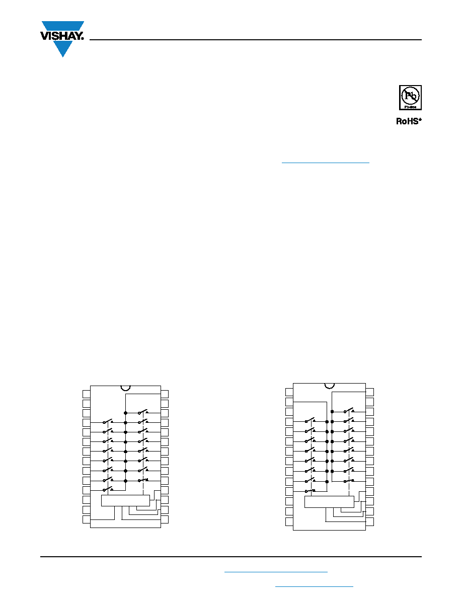
FUNCTIONAL BLOCK DIAGRAM AND PIN CONFIGURATION
Available
V+
S11
S10
S9
NC
A3
D
S2
S1
GND
A1
A2
NC
Dual-In-Line and SOIC Wide-Body
A0
EN
V-
NC
S8
S16
S7
S15
S6
S14
S5
S13
S4
S12
S3
1
2
3
4
5
6
7
8
28
27
26
25
24
23
22
21
Top View
920
10
19
11
12
18
17
13
16
14
15
DG406B
Decoders/Drivers
DG407B
V+
S3b
S2b
S1b
NC
Da
S2a
S1a
GND
A1
A2
Db
Dual-In-Line and SOIC Wide-Body
A0
EN
V-
NC
S8a
S8b
S7a
S7b
S6a
S6b
S5a
S5b
S4a
S4b
S3a
1
2
3
4
5
6
7
8
28
27
26
25
24
23
22
21
Top View
920
10
19
11
12
18
17
13
16
14
15
Decoders/Drivers
相关PDF资料 |
PDF描述 |
|---|---|
| VI-25X-IX-F3 | CONVERTER MOD DC/DC 5.2V 75W |
| PIC14000-20/SS | IC MCU OTP 4KX14 A/D 28SSOP |
| VI-20F-IX-F4 | CONVERTER MOD DC/DC 72V 75W |
| VI-20J-IX-F2 | CONVERTER MOD DC/DC 36V 75W |
| PIC18F6680-E/PT | IC PIC MCU FLASH 32KX16 64TQFP |
相关代理商/技术参数 |
参数描述 |
|---|---|
| DG406BDW | 功能描述:多路器开关 IC Single 16:1, 4-bit Multiplexer/MUX RoHS:否 制造商:Texas Instruments 通道数量:1 开关数量:4 开启电阻(最大值):7 Ohms 开启时间(最大值): 关闭时间(最大值): 传播延迟时间:0.25 ns 工作电源电压:2.3 V to 3.6 V 工作电源电流: 最大工作温度:+ 85 C 安装风格:SMD/SMT 封装 / 箱体:UQFN-16 |
| DG406BDW-E3 | 功能描述:多路器开关 IC Single 16:1, 4-bit Multiplexer/MUX RoHS:否 制造商:Texas Instruments 通道数量:1 开关数量:4 开启电阻(最大值):7 Ohms 开启时间(最大值): 关闭时间(最大值): 传播延迟时间:0.25 ns 工作电源电压:2.3 V to 3.6 V 工作电源电流: 最大工作温度:+ 85 C 安装风格:SMD/SMT 封装 / 箱体:UQFN-16 |
| DG406BP | 制造商:未知厂家 制造商全称:未知厂家 功能描述:GTO Thyristors - Disc / Puk Devices |
| DG406BP12 | 制造商:Dynex Semiconductor 功能描述:GTO THYRISTOR |
| DG406BP13 | 制造商:Dynex Semiconductor 功能描述:GTO THYRISTOR |
发布紧急采购,3分钟左右您将得到回复。