- 您现在的位置:买卖IC网 > PDF目录11270 > DG643DY-T1-E3 (Vishay Siliconix)IC VIDEO SWITCH SPDT 16SOIC PDF资料下载
参数资料
| 型号: | DG643DY-T1-E3 |
| 厂商: | Vishay Siliconix |
| 文件页数: | 13/18页 |
| 文件大小: | 0K |
| 描述: | IC VIDEO SWITCH SPDT 16SOIC |
| 标准包装: | 2,500 |
| 功能: | 视频开关 |
| 电路: | 2 x SPDT |
| 导通状态电阻: | 15 欧姆 |
| 电压电源: | 单/双电源 |
| 电压 - 电源,单路/双路(±): | 10 V ~ 18 V,±10 V ~ 15 V |
| 电流 - 电源: | 3.5mA |
| 工作温度: | -40°C ~ 85°C |
| 安装类型: | 表面贴装 |
| 封装/外壳: | 16-SOIC(0.154",3.90mm 宽) |
| 供应商设备封装: | 16-SOIC N |
| 包装: | 带卷 (TR) |
www.vishay.com
4
Document Number: 70058
S11-0154-Rev. F, 31-Jan-11
Vishay Siliconix
DG641, DG642, DG643
Notes:
a. Room = 25 °C, Full = as determined by the operating temperature suffix.
b. The algebraic convention whereby the most negative value is a minimum and the most positive a maximum, is used in this data sheet.
c. Typical values are for DESIGN AID ONLY, not guaranteed nor subject to production testing.
d. Guaranteed by design, not subject to production test.
e. VIN = input voltage to perform proper function.
Stresses beyond those listed under “Absolute Maximum Ratings” may cause permanent damage to the device. These are stress ratings only, and functional operation
of the device at these or any other conditions beyond those indicated in the operational sections of the specifications is not implied. Exposure to absolute maximum
rating conditions for extended periods may affect device reliability.
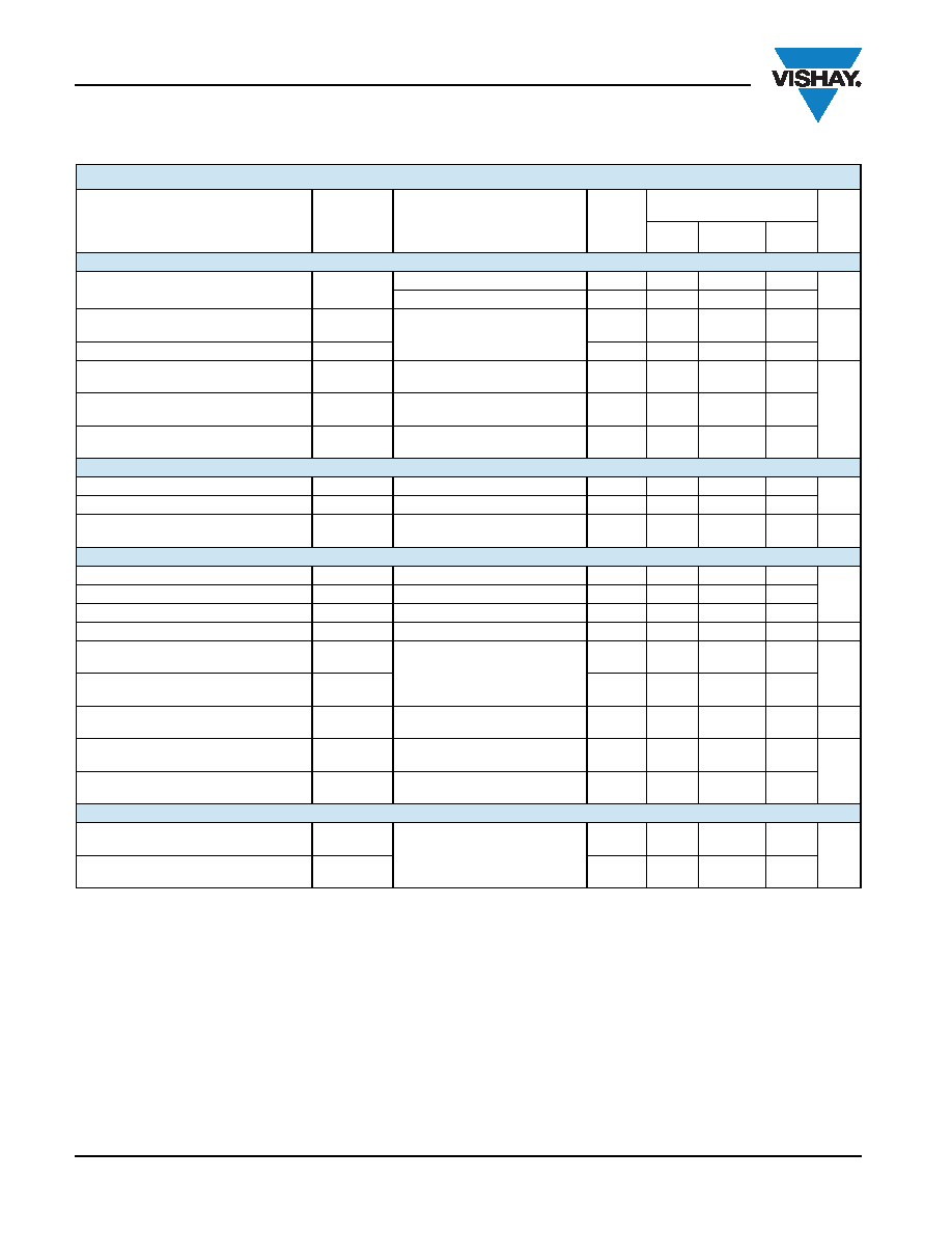
SPECIFICATIONS (for DG642)
Parameter
Symbol
Test Conditions
Unless Otherwise Specified
V+ = 15 V, V- = - 3 V
VINH = 2.4 V, VINL = 0.8 V
e
Temp.a
Limits
- 40 °C to 85 °C
Unit
Min.b
Typ.c
Max.b
Analog Switch
Analog Signal Ranged
VANALOG
V- = - 5 V, V+ = 12 V
Full
- 5
8
V
V- = GND V, V+ = 12 V
Full
0
8
Drain-Source On-Resistance
RDS(on)
IS = - 10 mA, VD = 0 V
Room
Full
58
9
RDS(on) Match
R
DS(on)
Room
0.5
1
Source Off Leakage Current
IS(off)
VS = 0 V, VD = 10 V
Room
Full
- 10
- 200
- 0.04
10
200
nA
Drain Off Leakage Current
ID(off)
VS = 10 V, VD = 0 V
Room
Full
- 10
- 200
- 0.04
10
200
Channel On Leakage Current
ID(on)
VS = VD = 0 V
Room
Full
- 10
- 200
- 0.2
10
200
Digital Control
Input Voltage High
VINH
Full
2.4
V
Input Voltage Low
VINL
Full
0.8
Input Current
IIN
VIN = GND or V+
Room
Full
- 1
- 20
0.05
1
20
A
Dynamic Characteristics
On State Input Capacitanced
CS(on)
VS = VD = 0 V
Room
19
40
pF
Off State Input Capacitanced
CS(off)
VD = 0 V
Room
8
20
Off State Output Capacitanced
CD(off)
VS = 0 V
Room
8
20
Bandwidth
BW
RL = 50 see figure 6
Room
500
MHz
Turn On Time
tON
RL = 1 kCL = 35 pF
see figure 2
Room
Full
60
100
160
ns
Turn Off Time
tOFF
Room
Full
40
60
100
Charge Injection
Q
CL = 1000 pF, VD = 0 V
see figure 3
Room
- 40
pC
Off Isolation
RIN = 75 RL = 75
f = 5 MHz, see figure 4
Room
- 63
dB
All Hostie Crosstalk
XTALK(AH)
RIN = 10 , RL = 75
f = 5 MHz, see figure 5
Room
- 85
Power Supplies
Positive Supply Current
I+
VIN = 0 V or VIN = 5 V
Room
Full
3.5
6
9
mA
Negative Supply Current
I-
Room
Full
- 6
- 9
- 3
相关PDF资料 |
PDF描述 |
|---|---|
| VI-253-IY-S | CONVERTER MOD DC/DC 24V 50W |
| GRM31CR61C226KE15K | CAP CER 22UF 16V 10% X5R 1206 |
| VE-2VN-IX-F2 | CONVERTER MOD DC/DC 18.5V 75W |
| GRM3197U1H472JZ01D | CAP CER 4700PF 50V 5% U2J 1206 |
| DSPIC30F6011AT-30I/PF | IC DSPIC MCU/DSP 132K 64TQFP |
相关代理商/技术参数 |
参数描述 |
|---|---|
| DG646BH | 制造商:未知厂家 制造商全称:未知厂家 功能描述:GTO Thyristors - Disc / Puk Devices |
| DG646BH25 | 制造商:Dynex Semiconductor 功能描述:GTO THYRISTOR |
| DG646BH25_05 | 制造商:DYNEX 制造商全称:Dynex Semiconductor 功能描述:Gate Turn-off Thyristor |
| DG646BH25-125A | 制造商:Dynex Semiconductor 功能描述:GTO THYRISTOR |
| DG646BH25-148 | 制造商:Dynex Semiconductor 功能描述:SCR - PHASE CONTROL THYRISTOR |
发布紧急采购,3分钟左右您将得到回复。