- 您现在的位置:买卖IC网 > PDF目录16767 > DP83848YB-EVK/NOPB (National Semiconductor)EVAL BOARD PHYTER EXTREME TEMP PDF资料下载
参数资料
| 型号: | DP83848YB-EVK/NOPB |
| 厂商: | National Semiconductor |
| 文件页数: | 16/86页 |
| 文件大小: | 0K |
| 描述: | EVAL BOARD PHYTER EXTREME TEMP |
| 标准包装: | 1 |
| 主要目的: | 接口,以太网 |
| 已用 IC / 零件: | DP83848YB |
| 已供物品: | 板 |
第1页第2页第3页第4页第5页第6页第7页第8页第9页第10页第11页第12页第13页第14页第15页当前第16页第17页第18页第19页第20页第21页第22页第23页第24页第25页第26页第27页第28页第29页第30页第31页第32页第33页第34页第35页第36页第37页第38页第39页第40页第41页第42页第43页第44页第45页第46页第47页第48页第49页第50页第51页第52页第53页第54页第55页第56页第57页第58页第59页第60页第61页第62页第63页第64页第65页第66页第67页第68页第69页第70页第71页第72页第73页第74页第75页第76页第77页第78页第79页第80页第81页第82页第83页第84页第85页第86页
www.national.com
22
D
P
838
48
YB
To tolerate potential frequency differences between the 50
MHz reference clock and the recovered receive clock, the
receive RMII function includes a programmable elasticity
buffer. The elasticity buffer is programmable to minimize
propagation delay based on expected packet size and
clock accuracy. This allows for supporting a range of
packet sizes including jumbo frames.
The elasticity buffer will force Frame Check Sequence
errors for packets which overrun or underrun the FIFO.
Underrun and Overrun conditions can be reported in the
RMII and Bypass Register (RBR). The following table indi-
cates how to program the elasticity buffer fifo (in 4-bit incre-
ments) based on expected max packet size and clock
accuracy. It assumes both clocks (RMII Reference clock
and far-end Transmitter clock) have the same accuracy.
3.3 10 Mb Serial Network Interface (SNI)
The DP83848YB incorporates a 10 Mb Serial Network
Interface (SNI) which allows a simple serial data interface
for 10 Mb only devices. This is also referred to as a 7-wire
interface. While there is no defined standard for this inter-
face, it is based on early 10 Mb physical layer devices.
Data is clocked serially at 10 MHz using separate transmit
and receive paths. The following pins are used in SNI
mode:
—TX_CLK
—TX_EN
—TXD[0]
—RX_CLK
—RXD[0]
— CRS
—COL
3.4 802.3u MII Serial Management Interface
3.4.1 Serial Management Register Access
The serial management MII specification defines a set of
thirty-two 16-bit status and control registers that are acces-
sible through the management interface pins MDC and
MDIO. The DP83848YB implements all the required MII
registers as well as several optional registers. These regis-
ters are fully described in Section 7.0. A description of the
serial management access protocol follows.
3.4.2 Serial Management Access Protocol
The serial control interface consists of two pins, Manage-
ment Data Clock (MDC) and Management Data Input/Out-
put (MDIO). MDC has a maximum clock rate of 25 MHz
and no minimum rate. The MDIO line is bi-directional and
may be shared by up to 32 devices. The MDIO frame for-
mat is shown below in Table 5.
The MDIO pin requires a pull-up resistor (1.5 k
) which,
during IDLE and turnaround, will pull MDIO high. In order to
initialize the MDIO interface, the station management entity
sends a sequence of 32 contiguous logic ones on MDIO to
provide the DP83848YB with a sequence that can be used
to establish synchronization. This preamble may be gener-
ated either by driving MDIO high for 32 consecutive MDC
clock cycles, or by simply allowing the MDIO pull-up resis-
tor to pull the MDIO pin high during which time 32 MDC
clock cycles are provided. In addition 32 MDC clock cycles
should be used to re-sync the device if an invalid start,
opcode, or turnaround bit is detected.
The DP83848YB waits until it has received this preamble
sequence before responding to any other transaction.
Once the DP83848YB serial management port has been
initialized no further preamble sequencing is required until
after a power-on/reset, invalid Start, invalid Opcode, or
invalid turnaround bit has occurred.
The Start code is indicated by a <01> pattern. This assures
the MDIO line transitions from the default idle line state.
Turnaround is defined as an idle bit time inserted between
the Register Address field and the Data field. To avoid con-
tention during a read transaction, no device shall actively
drive the MDIO signal during the first bit of Turnaround.
The addressed DP83848YB drives the MDIO with a zero
for the second bit of turnaround and follows this with the
required data. Figure 4 shows the timing relationship
between MDC and the MDIO as driven/received by the Sta-
tion (STA) and the DP83848YB (PHY) for a typical register
read access.
For write transactions, the station management entity
writes data to the addressed DP83848YB thus eliminating
the requirement for MDIO Turnaround. The Turnaround
time is filled by the management entity by inserting <10>.
Figure 5 shows the timing relationship for a typical MII reg-
ister write access.
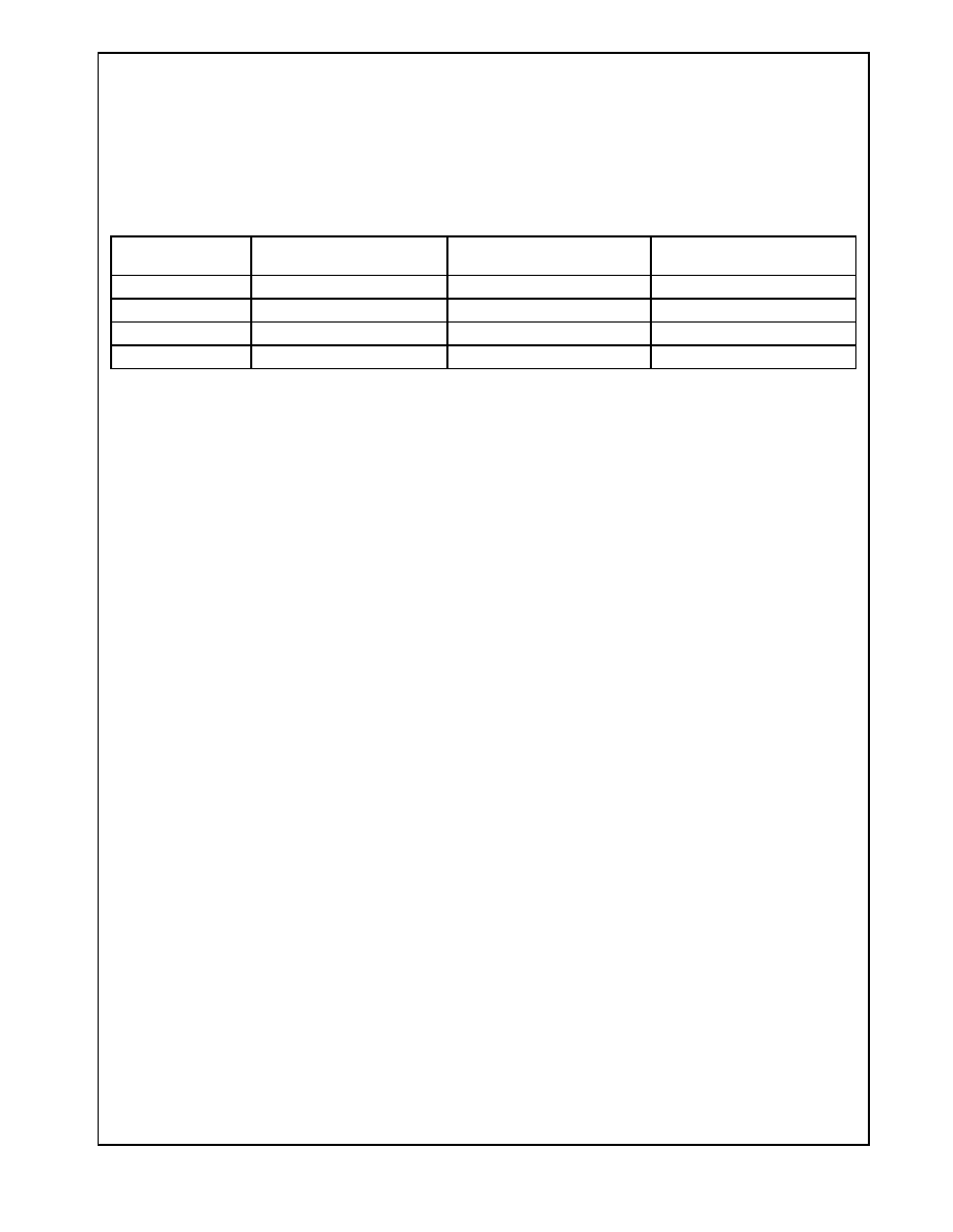
Table 4. Supported packet sizes at +/-50ppm +/-100ppm for each clock
Start Threshold
RBR[1:0]
Latency Tolerance
Recommended Packet Size
at +/- 50ppm
Recommended Packet Size at
+/- 100ppm
1 (4-bits)
2 bits
2400 bytes
1200 bytes
2 (8-bits)
6 bits
7200 bytes
3600 bytes
3 (12-bits)
10 bits
12000 bytes
6000 bytes
0 (16-bits)
14 bits
16800 bytes
8400 bytes
相关PDF资料 |
PDF描述 |
|---|---|
| 200LLE8R2MEFC8X9 | CAP ALUM 8.2UF 200V 20% RADIAL |
| 462A423-51-0 | BOOT MOLDED |
| M3DDA-1636J | IDC CABLE - MKR16A/MC16G/MKR16A |
| 0210200344 | CABLE FLAT FLEX 4" 0.50MM 32POS |
| UPJ1V390MED1TD | CAP ALUM 39UF 35V 20% RADIAL |
相关代理商/技术参数 |
参数描述 |
|---|---|
| DP83848YBX/NOPB | 功能描述:以太网 IC RoHS:否 制造商:Micrel 产品:Ethernet Switches 收发器数量:2 数据速率:10 Mb/s, 100 Mb/s 电源电压-最大:1.25 V, 3.45 V 电源电压-最小:1.15 V, 3.15 V 最大工作温度:+ 85 C 封装 / 箱体:QFN-64 封装:Tray |
| DP83849C | 制造商:NSC 制造商全称:National Semiconductor 功能描述:PHYTER? DUAL Commercial Temperature Dual Port 10/100 Mb/s Ethernet Physical Layer Transceiver |
| DP83849C_08 | 制造商:NSC 制造商全称:National Semiconductor 功能描述:PHYTER? DUAL Commercial Temperature Dual Port 10/100 Mb/s Ethernet Physical Layer Transceiver |
| DP83849CVS | 功能描述:以太网 IC RoHS:否 制造商:Micrel 产品:Ethernet Switches 收发器数量:2 数据速率:10 Mb/s, 100 Mb/s 电源电压-最大:1.25 V, 3.45 V 电源电压-最小:1.15 V, 3.15 V 最大工作温度:+ 85 C 封装 / 箱体:QFN-64 封装:Tray |
| DP83849CVS | 制造商:Texas Instruments 功能描述:TRANSCEIVER, ENET PHYTER, DUAL, 80TQFP 制造商:Texas Instruments 功能描述:TRANSCEIVER, ENET PHYTER, DUAL, 80TQFP; Data Rate:100Mbps; Ethernet Type:IEEE 802.3u; Supply Voltage Min:3V; Supply Voltage Max:3.6V; Digital IC Case Style:TQFP; No. of Pins:80; Interface Type:MII, RMII, Serial; Operating Temperature;RoHS Compliant: Yes |
发布紧急采购,3分钟左右您将得到回复。