- 您现在的位置:买卖IC网 > PDF目录171220 > DPZ128X16IHY-17M (TWILIGHT TECHNOLOGY INC) 128K X 16 FLASH 12V PROM MODULE, 170 ns, QFP48 PDF资料下载
参数资料
| 型号: | DPZ128X16IHY-17M |
| 厂商: | TWILIGHT TECHNOLOGY INC |
| 元件分类: | PROM |
| 英文描述: | 128K X 16 FLASH 12V PROM MODULE, 170 ns, QFP48 |
| 封装: | HERMETIC SEALED, CERAMIC, GULLWING, MODULE, SLCC-48 |
| 文件页数: | 11/16页 |
| 文件大小: | 1082K |
| 代理商: | DPZ128X16IHY-17M |
DPZ128X16IY/IIY/IJY/IHY/IA3
Dense-Pac Microsystems, Inc.
device, it indicates the location is erased. The erase/verify
command is issued prior to each location verification to latch
the address of the location to be verified. This continues until
FFH is not read from the device or the last address for the
device being erased is read.
If FFH is not read from the location being verified, an
additional erase operation is performed. Verification then
resumes from the last location verified. Once all locations in
the device being erased are verified, the erase operation is
complete. The verify operation should now be terminated by
writing a valid command such as program set-up to the
command register.
PRODUCT I.D. OPERATION:
The product I.D. operation outputs the manufacturer code
(89H) and the device code (B4H). This allows programming
equipment to match the device with the proper erase and
programming algorithms.
With CE and OE at a logic low level, raising A9 to VID (see
DC Operating Characteristics)
will initiate the operation. The
manufacturer’s code can then be read from address location
0000H and the device code can be read from address
location 0001H.
The I.D. codes can also be accessed via the command
register. Following a write of 90H to the command register,
a read from address location 0000H outputs the
manufacturer’s code (89H). A read from address location
0001H outputs the device code (B4H). To terminate the
operation, it is necessary to write another valid command into
the register.
POWER UP/DOWN PROTECTION:
The FLASH devices are designed to protect against accidental
erasure or programming during power transitions. It makes
no difference as to which power supply, VPP or VDD, powers
up first. Power supply sequencing is not required. Internal
circuitry ensures that the command register is reset to the read
mode upon power up.
POWER SUPPLY DECOUPLING:
VPP traces should use trace widths and layout considerations
comparable to that of the VDD power bus. The VPP supply
traces should also be decoupled to help decrease voltage
spikes.
While the memory module has high-frequency,
low-inductance decoupling capacitors mounted on the
substrate connected to VDD and VSS, it is recommended that
a 4.7
F to 10F electrolytic capacitor be placed near the
memory module connected across VDD and VSS for bulk
storage. Decoupling capacitors should also be placed near
the module, connected across VPP and VSS.
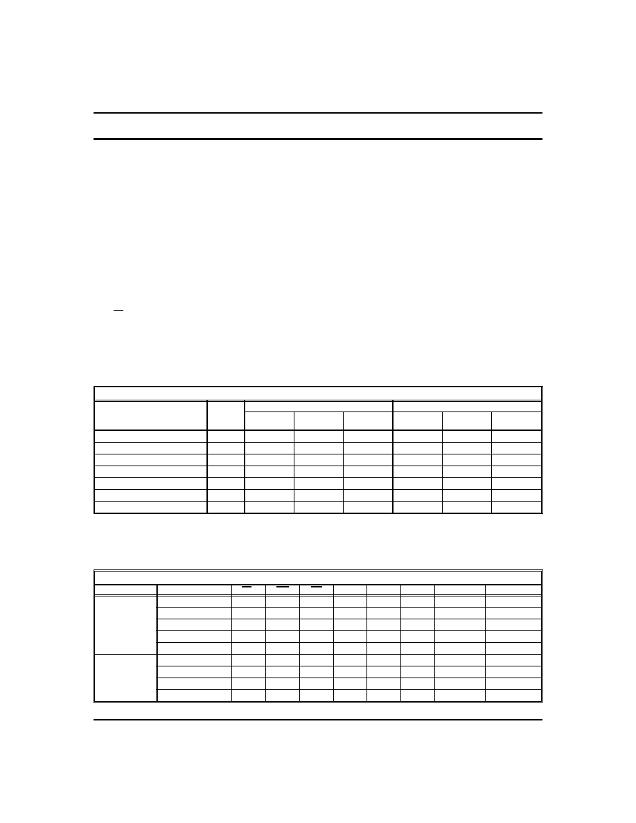
COMMAND DEFINITION TABLE
Command
Bus
Cycles
Req’d
First Bus Cycle
Second Bus Cycle
Operation
Address
Data
1
Operation
Address
Data
1
Read Memory
1
Write
X
00H
-
Setup Erase / Erase
2
Write
X
20H
Write
X
20H
Erase Verify
2
Write
EA
A0H
Read
X
EVD
Setup Program / Program
2
Write
X
40H
Write
PA
PD
Program Verify
2
Write
X
C0H
Read
X
PVD
Reset
2
Write
X
FFH
Write
X
FFH
Read Product I.D. Codes
3
Write
X
90H
Read
IA
ID
EA = Address to Verify
PA = Address to Program
EVD = Data Read from Location EA
PD = Data to be Programmed at Location PA
IA
= Address: 0000H for manufacturing code, 0001H for device code
PVA = Data to be Read from Location PA at Program Verify
ID = ID data read from IA during product ID operation
(Manufacturer = 89H, Device = B4H)
TRUTH TABLE
Mode
Description
CEn
WE
OE
A0
A9
VPP
I/O Pins
Supply Current
READ
ONLY
Not Selected
H
X
VPPLO
HIGH-Z
Standby
Output Disable
L
H
X
VPPLO
HIGH-Z
Active
Read
L
H
L
A0
A9
VPPLO
DOUT
Active
I.D. (Mfr.)
L
H
L
VID
VPPLO
DOUT =89H
Active
I.D. (Device)
L
H
L
H
VID
VPPLO
DOUT = B4H
Active
COMMAND
PROGRAM
Not Selected
H
X
VPPHI
HIGH-Z
Standby
Output Disable
L
H
X
VPPHI
HIGH-Z
Active
Read
L
H
L
A0
A9
VPPHI
DOUT
Active
Write
L
H
A0
A9
VPPHI
DIN
Active
30A071-13
REV. D
4
相关PDF资料 |
PDF描述 |
|---|---|
| DPZ128X32VI-25M | 512K X 8 FLASH 12V PROM MODULE, 250 ns, CPGA66 |
| DQ1260-680M-B | 1 ELEMENT, 68 uH, GENERAL PURPOSE INDUCTOR, SMD |
| DQ1280-4R7M-B | 1 ELEMENT, 4.7 uH, GENERAL PURPOSE INDUCTOR, SMD |
| DQ6530-150M | 1 ELEMENT, 15 uH, GENERAL PURPOSE INDUCTOR, SMD |
| DQ6530-221M-B | 1 ELEMENT, 220 uH, GENERAL PURPOSE INDUCTOR, SMD |
相关代理商/技术参数 |
参数描述 |
|---|---|
| DQ1001-7R | 制造商:Power-One 功能描述:DC/DC PS SGL-OUT 5.1V 20A 102W - Bulk |
| DQ1001-9R | 功能描述:EURO-CASSETTE 82W 5.1V RoHS:否 类别:电源 - 外部/内部(非板载) >> DC DC Converters 系列:* 标准包装:1 系列:Quint 类型:隔离 输入电压:24V 输出:24V 输出数:1 输出 - 1 @ 电流(最大):24 VDC @ 50A 输出 - 2 @ 电流(最大):- 输出 - 3 @ 电流(最大):- 输出 - 4 @ 电流(最大):- 功率(瓦特):1200W 安装类型:底座安装 工作温度:0°C ~ 40°C 效率:- 封装/外壳:模块 尺寸/尺寸:4.33" L x 9.09" W x 6.14" H(110mm x 231mm x 156mm) 包装:散装 电源(瓦特)- 最大:1200W 批准:- 其它名称:277-69722866365-NDQUINT-BAT/24DC/12AH |
| DQ1101-7 | 制造商:Power-One 功能描述:DC/DC PS SGL-OUT 3.3V 25A 82W - Bulk |
| DQ1101-9 | 功能描述:EURO-CASSETTE 66W 3.3V RoHS:否 类别:电源 - 外部/内部(非板载) >> DC DC Converters 系列:* 标准包装:1 系列:Quint 类型:隔离 输入电压:24V 输出:24V 输出数:1 输出 - 1 @ 电流(最大):24 VDC @ 50A 输出 - 2 @ 电流(最大):- 输出 - 3 @ 电流(最大):- 输出 - 4 @ 电流(最大):- 功率(瓦特):1200W 安装类型:底座安装 工作温度:0°C ~ 40°C 效率:- 封装/外壳:模块 尺寸/尺寸:4.33" L x 9.09" W x 6.14" H(110mm x 231mm x 156mm) 包装:散装 电源(瓦特)- 最大:1200W 批准:- 其它名称:277-69722866365-NDQUINT-BAT/24DC/12AH |
| DQ1260 | 制造商:MA-COM 制造商全称:M/A-COM Technology Solutions, Inc. 功能描述:SMD Shielded Base Plate Power Inductor Series |
发布紧急采购,3分钟左右您将得到回复。