- 您现在的位置:买卖IC网 > PDF目录378586 > DS1244W-120IND 256k NV SRAM with Phantom Clock PDF资料下载
参数资料
| 型号: | DS1244W-120IND |
| 英文描述: | 256k NV SRAM with Phantom Clock |
| 中文描述: | 256k非易失SRAM与幻影时钟 |
| 文件页数: | 8/19页 |
| 文件大小: | 292K |
| 代理商: | DS1244W-120IND |
ADS1244
SBAS273
8
www.ti.com
VOLTAGE REFERENCE INPUTS (VREFP, VREFN)
The voltage reference used by the modulator is generated
from the voltage difference between VREFP and VREFN:
V
REF
= VREFP
–
VREFN. The reference inputs use a structure
similar to that of the analog inputs. A simplified diagram of the
circuitry on the reference inputs is shown in Figure 5. The
switches and capacitors can be modeled with an effective
impedance =
t
pF
SAMPLE
2
25
/
= 1M
for f
CLK
= 2.4576MHz.
Minimize the overshoot and undershoot on CLK for the best
analog performance. A small resistor in series with CLK (10
to 100
) can often help. CLK can be generated from a number
of sources including stand-alone crystal oscillators and
microcontrollers. The MSP430, an ultra low power
microcontroller, is especially well suited for this task. Using the
MSP430
’
s FLL clock generator available on the 4xx family, it
’
s
easy to produce a 2.4576MHz clock from a 32.768kHz crystal.
DATA READY/DATA OUTPUT (
DRDY/DOUT
)
This digital output pin serves two purposes. It indicates when
new data is ready by going LOW. Afterwards, on the first rising
edge of SCLK, the
DRDY/DOUT
pin changes function and
begins outputting the conversion data, MSB first. Data is
shifted out on each subsequent SCLK rising edge. After all 24
bits have been retrieved, the pin can be forced HIGH with an
additional SCLK. It will then stay HIGH until new data is ready.
This is useful when polling on the status of
DRDY/DOUT
to
determine when to begin data retrieval.
SERIAL CLOCK INPUT (SCLK)
This digital input shifts serial data out with each rising edge.
As with CLK, this input may be driven with 5V logic regard-
less of the DVDD or AVDD voltage. There is hysteresis built
into this input, but care should still be taken to ensure a clean
signal. Glitches or slow rising signals can cause unwanted
additional shifting. For this reason, it is best to make sure the
rise-and-fall times of SCLK are less than 50ns.
FREQUENCY RESPONSE
The ADS1244
’
s frequency response for f
CLK
= 2.4576MHz is
shown in Figure 6. The frequency response repeats at mul-
tiples of 19.2kHz. The overall response is that of a low-pass
filter with a
–
3dB cutoff frequency of 13.7Hz. As can be seen,
the ADS1244 does a good job attenuating out to 19kHz. For
the best resolution, limit the input bandwidth to below this value
to keep higher frequency noise from affecting performance.
Often a simple RC filter on the ADS1244
’
s analog inputs is all
that is needed.
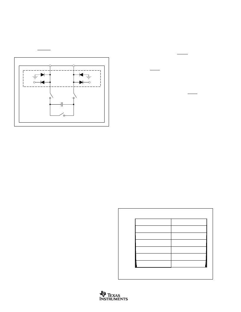
FIGURE 5. Simplified Reference Input Circuitry.
25pF
S
2
S
1
S
1
AVDD
VREFP
VREFN
AVDD
ESD
Protection
ESD diodes protect the reference inputs. To prevent
these diodes from turning on, make sure the voltages on
the reference pins do not go below GND by more than
100mV, and likewise do not exceed AVDD by 100mV:
GND
–
100mV < (VREFP, VREFN) < AVDD + 100mV.
V
REF
is typically AVDD/2, but it can be raised as high as
AVDD. When V
REF
exceeds AVDD/2, it will not be possible
to reach the full-scale digital output value corresponding to
±
2V
REF
since this would require the analog inputs to exceed
the power supplies.
For example, if V
REF
= AVDD = 5V, the
positive full-scale signal is 10V. The maximum positive input
signal that can be supplied before the ESD diodes begin to turn
on is when AINP = 5.1V and AINN =
–
0.1V
→
V
IN
= 5.2V.
Therefore, it will not be possible to reach the positive (or
negative) full-scale readings in this configuration. The digital
output codes will be limited to approximately one half of the
entire range.
For best performance, bypass the voltage reference inputs
with a 0.1
μ
F capacitor between VREFP and VREFN. Place
the capacitor as close as possible to the pins.
CLOCK INPUT (CLK)
This digital input supplies the system clock to the ADS1244.
The recommended CLK frequency is 2.4576MHz. This places
the notches of the digital filter at 50Hz and 60Hz and sets the
data rate at 15SPS. The CLK frequency can be increased to
speed up the data rate, but the frequency notches will move
in frequency proportionally. CLK must be left running during
normal operation. It may be turned off during Sleep Mode to
save power, but this is not required. The CLK input may be
driven with 5V logic, regardless of the DVDD or AVDD voltage.
FIGURE 6. Frequency Response.
FREQUENCY RESPONSE
f
CLK
= 2.4576MHz
Frequency (kHz)
G
9.6
19.2
0
0
–
20
–
40
–
60
–
80
–
100
–
120
–
140
相关PDF资料 |
PDF描述 |
|---|---|
| DS1244WP-120IND | 256k NV SRAM with Phantom Clock |
| DS1244YP-70 | CAT5E PATCH CORD 30 FOOT BEIGE |
| DS1244Y-70 | 256k NV SRAM with Phantom Clock |
| DS1244W-120 | 256k NV SRAM with Phantom Clock |
| DS1244WP-120 | 256k NV SRAM with Phantom Clock |
相关代理商/技术参数 |
参数描述 |
|---|---|
| DS1244W-120IND+ | 功能描述:实时时钟 256k NV SRAM w/Phantom Clock RoHS:否 制造商:Microchip Technology 功能:Clock, Calendar. Alarm RTC 总线接口:I2C 日期格式:DW:DM:M:Y 时间格式:HH:MM:SS RTC 存储容量:64 B 电源电压-最大:5.5 V 电源电压-最小:1.8 V 最大工作温度:+ 85 C 最小工作温度: 安装风格:Through Hole 封装 / 箱体:PDIP-8 封装:Tube |
| DS1244WP-120 | 功能描述:实时时钟 RoHS:否 制造商:Microchip Technology 功能:Clock, Calendar. Alarm RTC 总线接口:I2C 日期格式:DW:DM:M:Y 时间格式:HH:MM:SS RTC 存储容量:64 B 电源电压-最大:5.5 V 电源电压-最小:1.8 V 最大工作温度:+ 85 C 最小工作温度: 安装风格:Through Hole 封装 / 箱体:PDIP-8 封装:Tube |
| DS1244WP-120+ | 功能描述:实时时钟 256k NV SRAM w/Phantom Clock RoHS:否 制造商:Microchip Technology 功能:Clock, Calendar. Alarm RTC 总线接口:I2C 日期格式:DW:DM:M:Y 时间格式:HH:MM:SS RTC 存储容量:64 B 电源电压-最大:5.5 V 电源电压-最小:1.8 V 最大工作温度:+ 85 C 最小工作温度: 安装风格:Through Hole 封装 / 箱体:PDIP-8 封装:Tube |
| DS1244WP-120IND | 功能描述:IC NVSRAM 256KBIT 120NS 34PCM RoHS:否 类别:集成电路 (IC) >> 时钟/计时 - 实时时钟 系列:- 产品培训模块:Obsolescence Mitigation Program 标准包装:1 系列:- 类型:时钟/日历 特点:警报器,闰年,SRAM 存储容量:- 时间格式:HH:MM:SS(12/24 小时) 数据格式:YY-MM-DD-dd 接口:SPI 电源电压:2 V ~ 5.5 V 电压 - 电源,电池:- 工作温度:-40°C ~ 85°C 安装类型:表面贴装 封装/外壳:8-WDFN 裸露焊盘 供应商设备封装:8-TDFN EP 包装:管件 |
| DS1244WP-120IND+ | 功能描述:实时时钟 256k NV SRAM w/Phantom Clock RoHS:否 制造商:Microchip Technology 功能:Clock, Calendar. Alarm RTC 总线接口:I2C 日期格式:DW:DM:M:Y 时间格式:HH:MM:SS RTC 存储容量:64 B 电源电压-最大:5.5 V 电源电压-最小:1.8 V 最大工作温度:+ 85 C 最小工作温度: 安装风格:Through Hole 封装 / 箱体:PDIP-8 封装:Tube |
发布紧急采购,3分钟左右您将得到回复。