- 您现在的位置:买卖IC网 > PDF目录1993 > DS12C887A+ (Maxim Integrated Products)IC RTC W/RAM 128 BYTE 24-EDIP PDF资料下载
参数资料
| 型号: | DS12C887A+ |
| 厂商: | Maxim Integrated Products |
| 文件页数: | 4/22页 |
| 文件大小: | 0K |
| 描述: | IC RTC W/RAM 128 BYTE 24-EDIP |
| 产品培训模块: | Lead (SnPb) Finish for COTS Obsolescence Mitigation Program |
| 标准包装: | 14 |
| 类型: | 时钟/日历 |
| 特点: | 警报器,夏令时,闰年,NVSRAM,方波输出 |
| 存储容量: | 113B |
| 时间格式: | HH:MM:SS(12/24 小时) |
| 数据格式: | YY-MM-DD-dd |
| 接口: | 并联 |
| 电源电压: | 4.5 V ~ 5.5 V |
| 电压 - 电源,电池: | 2.5 V ~ 4 V |
| 工作温度: | 0°C ~ 70°C |
| 安装类型: | 通孔 |
| 封装/外壳: | 24-DIP 模块(0.600",15.24mm) |
| 供应商设备封装: | 24-EDIP |
| 包装: | 管件 |
| 产品目录页面: | 1433 (CN2011-ZH PDF) |
DS12885/DS12887/DS12887A/DS12C887/DS12C887A
Real-Time Clocks
12
____________________________________________________________________
Clock Accuracy
The accuracy of the clock is dependent upon the accu-
racy of the crystal and the accuracy of the match
between the capacitive load of the oscillator circuit and
the capacitive load for which the crystal was trimmed.
Additional error is added by crystal frequency drift
caused by temperature shifts. External circuit noise cou-
pled into the oscillator circuit can result in the clock run-
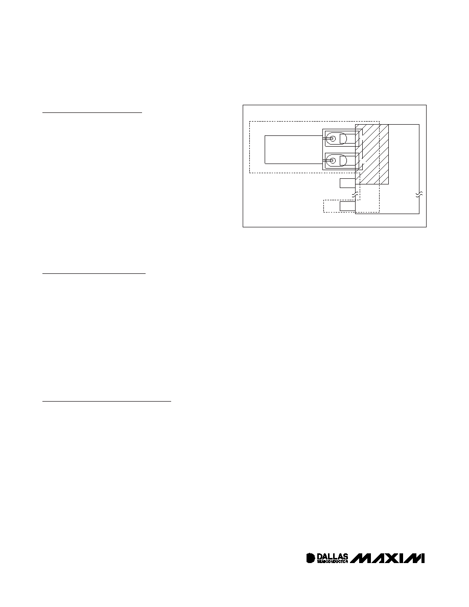
ning fast. Figure 2 shows a typical PC board layout for
isolation of the crystal and oscillator from noise. Refer to
Application Note 58: Crystal Considerations with Dallas
Real-Time Clocks for more detailed information.
Clock Accuracy for DS12887, DS12887A,
DS12C887, DS12C887A Only
The encapsulated DIP modules are trimmed at the fac-
tory to an accuracy of ±1 minute per month at +25°C.
Power-Down/Power-Up
Considerations
The real-time clock continues to operate, and the RAM,
time, calendar, and alarm memory locations remain
nonvolatile regardless of the VCC input level. VBAT must
remain within the minimum and maximum limits when
VCC is not applied. When VCC is applied and exceeds
VPF (power-fail trip point), the device becomes accessi-
ble after tREC—if the oscillator is running and the oscil-
lator countdown chain is not in reset (Register A). This
time allows the system to stablize after power is
applied. If the oscillator is not enabled, the oscillator-
enable bit is enabled on power-up, and the device
becomes immediately accessible.
Time, Calendar, and Alarm
Locations
The time and calendar information is obtained by read-
ing the appropriate register bytes. The time, calendar,
and alarm are set or initialized by writing the appropri-
ate register bytes. Invalid time or date entries result in
undefined operation. The contents of the 10 time, cal-
endar, and alarm bytes can be either binary or binary-
coded decimal (BCD) format.
The day-of-week register increments at midnight, incre-
menting from 1 through 7. The day-of-week register is
used by the daylight saving function, so the value 1 is
defined as Sunday. The date at the end of the month is
automatically adjusted for months with fewer than 31
days, including correction for leap years.
Before writing the internal time, calendar, and alarm reg-
isters, the SET bit in Register B should be written to logic
1 to prevent updates from occurring while access is
being attempted. In addition to writing the 10 time, calen-
dar, and alarm registers in a selected format (binary or
BCD), the data mode bit (DM) of Register B must be set
to the appropriate logic level. All 10 time, calendar, and
alarm bytes must use the same data mode. The SET bit
in Register B should be cleared after the data mode bit
has been written to allow the RTC to update the time and
calendar bytes. Once initialized, the RTC makes all
updates in the selected mode. The data mode cannot be
changed without reinitializing the 10 data bytes. Tables
2A and 2B show the BCD and binary formats of the time,
calendar, and alarm locations.
The 24-12 bit cannot be changed without reinitializing the
hour locations. When the 12-hour format is selected, the
higher-order bit of the hours byte represents PM when it
is logic 1. The time, calendar, and alarm bytes are always
accessible because they are double-buffered. Once per
second the seven bytes are advanced by one second
and checked for an alarm condition.
If a read of the time and calendar data occurs during
an update, a problem exists where seconds, minutes,
hours, etc., may not correlate. The probability of read-
ing incorrect time and calendar data is low. Several
methods of avoiding any possible incorrect time and
calendar reads are covered later in this text.
LOCAL GROUND PLANE (TOP LAYER)
CRYSTAL
GND
X2
X1
NOTE: AVOID ROUTING SIGNAL LINES
IN THE CROSSHATCHED AREA
(UPPER LEFT QUADRANT) OF
THE PACKAGE UNLESS THERE IS
A GROUND PLANE BETWEEN THE
SIGNAL LINE AND THE DEVICE PACKAGE.
Figure 2. Layout Example
相关PDF资料 |
PDF描述 |
|---|---|
| DS12CR887-5+ | IC RTC W/RAM 128 BYTE 24-EDIP |
| DS1302SN-16 | IC TIMEKEEPER T-CHRG IND 16-SOIC |
| DS1305E/T&R | IC RTC SERIAL ALARM 20-TSSOP |
| DS1306EN/T&R | IC RTC SERIAL ALARM IND 20-TSSOP |
| DS1307N | IC RTC SERIAL 512K IND 8-DIP |
相关代理商/技术参数 |
参数描述 |
|---|---|
| DS12C887A+ | 功能描述:实时时钟 RTC RoHS:否 制造商:Microchip Technology 功能:Clock, Calendar. Alarm RTC 总线接口:I2C 日期格式:DW:DM:M:Y 时间格式:HH:MM:SS RTC 存储容量:64 B 电源电压-最大:5.5 V 电源电压-最小:1.8 V 最大工作温度:+ 85 C 最小工作温度: 安装风格:Through Hole 封装 / 箱体:PDIP-8 封装:Tube |
| DS12CR887-33 | 功能描述:实时时钟 RoHS:否 制造商:Microchip Technology 功能:Clock, Calendar. Alarm RTC 总线接口:I2C 日期格式:DW:DM:M:Y 时间格式:HH:MM:SS RTC 存储容量:64 B 电源电压-最大:5.5 V 电源电压-最小:1.8 V 最大工作温度:+ 85 C 最小工作温度: 安装风格:Through Hole 封装 / 箱体:PDIP-8 封装:Tube |
| DS12CR887-33+ | 功能描述:实时时钟 RTC w/Constant V Trickle Charger RoHS:否 制造商:Microchip Technology 功能:Clock, Calendar. Alarm RTC 总线接口:I2C 日期格式:DW:DM:M:Y 时间格式:HH:MM:SS RTC 存储容量:64 B 电源电压-最大:5.5 V 电源电压-最小:1.8 V 最大工作温度:+ 85 C 最小工作温度: 安装风格:Through Hole 封装 / 箱体:PDIP-8 封装:Tube |
| DS12CR887-5 | 功能描述:实时时钟 RoHS:否 制造商:Microchip Technology 功能:Clock, Calendar. Alarm RTC 总线接口:I2C 日期格式:DW:DM:M:Y 时间格式:HH:MM:SS RTC 存储容量:64 B 电源电压-最大:5.5 V 电源电压-最小:1.8 V 最大工作温度:+ 85 C 最小工作温度: 安装风格:Through Hole 封装 / 箱体:PDIP-8 封装:Tube |
| DS12CR887-5+ | 功能描述:实时时钟 RTC w/Constant V Trickle Charger RoHS:否 制造商:Microchip Technology 功能:Clock, Calendar. Alarm RTC 总线接口:I2C 日期格式:DW:DM:M:Y 时间格式:HH:MM:SS RTC 存储容量:64 B 电源电压-最大:5.5 V 电源电压-最小:1.8 V 最大工作温度:+ 85 C 最小工作温度: 安装风格:Through Hole 封装 / 箱体:PDIP-8 封装:Tube |
发布紧急采购,3分钟左右您将得到回复。