参数资料
| 型号: | DS1314S/T&R |
| 厂商: | Maxim Integrated |
| 文件页数: | 8/12页 |
| 文件大小: | 0K |
| 描述: | IC CTRLR NV W/BATT MON 3V 16SOIC |
| 产品培训模块: | Lead (SnPb) Finish for COTS Obsolescence Mitigation Program |
| 标准包装: | 1,000 |
| 控制器类型: | 非易失性 RAM |
| 电源电压: | 3 V ~ 3.6 V |
| 工作温度: | -40°C ~ 85°C |
| 封装/外壳: | 16-SOIC(0.295",7.50mm 宽) |
| 供应商设备封装: | 16-SOIC W |
| 包装: | 带卷 (TR) |
DS1314
5 of 12
ABSOLUTE MAXIMUM RATINGS
Voltage Range on Any Pin Relative to Ground
-0.5V to +6.0V
Operating Temperature Range
-40°C to +85°C
Storage Temperature Range
-55°C to +125°C
Soldering Temperature (reflow, SO or TSSOP)
+260°C
Lead Temperature (soldering, 10s)
+300°C
This is a stress rating only and functional operation of the device at these or any other conditions above those indicated in the
operation sections of this specification is not implied. Exposure to absolute maximum rating conditions for extended periods of
time may affect reliability.
PACKAGE THERMAL CHARACTERISTICS (Note 1)
PDIP
Junction-to-Ambient Thermal Resistance (θJA).…………………...………………………....110°C/W
Junction-to-Case Thermal Resistance (θJC)……………………………………………………40°C/W
8 SO
Junction-to-Ambient Thermal Resistance (θJA).……………………………………………...132°C/W
Junction-to-Case Thermal Resistance (θJC)……………………………………………………38°C/W
16 SO
Junction-to-Ambient Thermal Resistance (θJA).…………………...………………………......71°C/W
Junction-to-Case Thermal Resistance (θJC)……………………………………………………23°C/W
TSSOP
Junction-to-Ambient Thermal Resistance (θJA).……………………………………………..73.8°C/W
Junction-to-Case Thermal Resistance (θJC)……………………………………………………20°C/W
Note 1:
Package thermal resistances were obtained using the method described in JEDEC specification JESD51-7, using a four-layer
board for the SMT packages. For detailed information on package thermal considerations, refer to
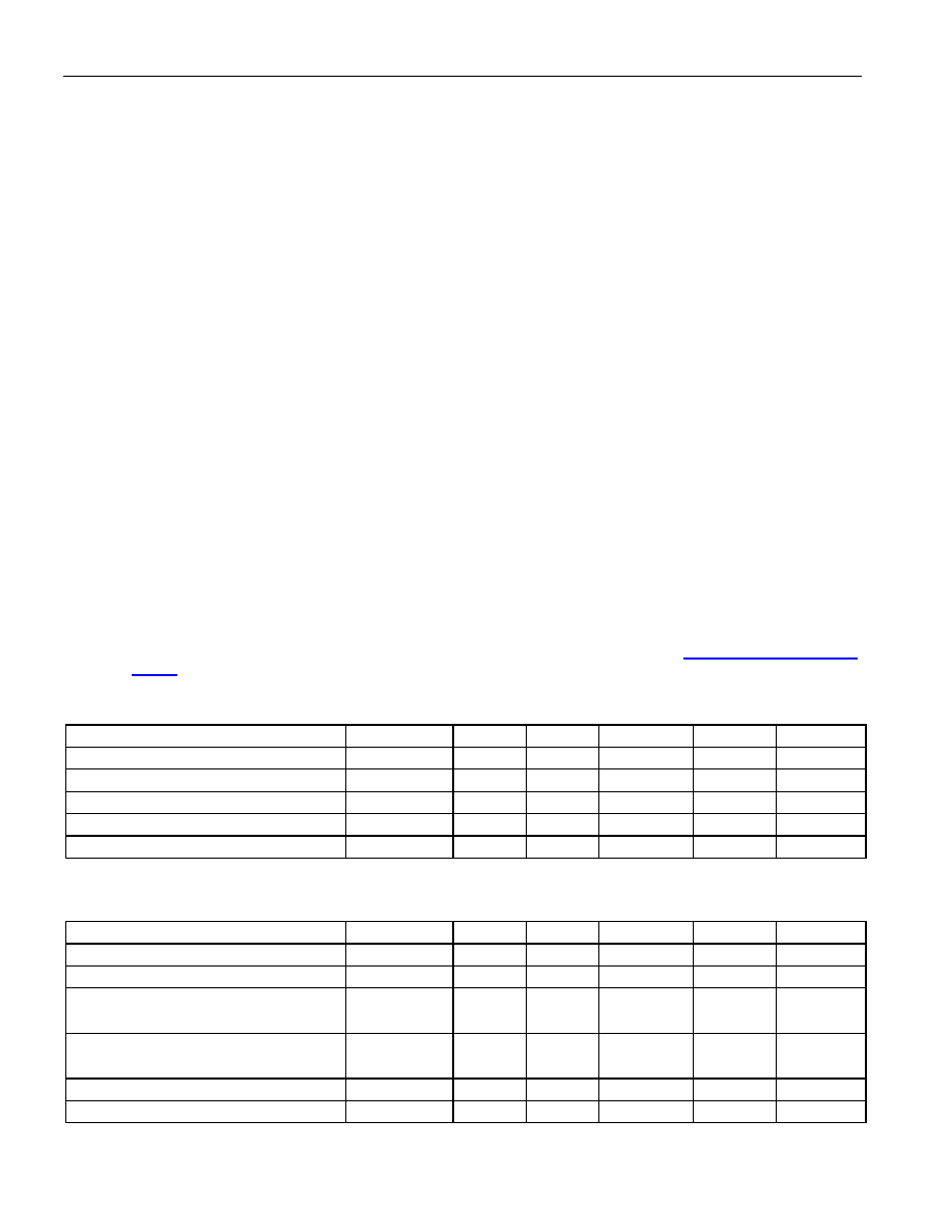
RECOMMENDED OPERATING CONDITIONS
(-40°C to +85°C)
PARAMETER
SYMBOL
MIN
TYP
MAX
UNITS
NOTES
Supply Voltage TOL=GND
VCCI
3.0
3.3
3.6
V
2
Supply Voltage TOL=VCCO
VCCI
2.7
3.0
3.3
V
2
Battery Supply Voltage
VBAT
2.0
6.0
V
2
Logic 1 Input
VIH
2.0
VCCI+0.3
V
2, 13
Logic 0 Input
VIL
-0.3
+0.8
V
2, 13
DC ELECTRICAL CHARACTERISTICS
(-40°C to +85°C; VCCI = ≥VCCTP)
PARAMETER
SYMBOL
MIN
TYP
MAX
UNITS
NOTES
Operating Current (TTL inputs)
ICC1
50
200
A
3
Operating Current (CMOS inputs)
ICC2
30
100
A
3, 6
RAM Supply Current
(VCCO ≥ VCCI -0.2V)
ICCO1
80
mA
4
RAM Supply Current
(VCCO ≥ VCCI -0.3V)
ICCO1
140
mA
5
VCC Trip Point (TOL=GND)
VCCTP
2.8
2.9
3.0
V
2
VCC Trip Point (TOL=VCCO)
VCCTP
2.5
2.6
2.7
V
2
相关PDF资料 |
PDF描述 |
|---|---|
| DS1321E/T&R | IC CTRL NV W/BATT MON 5V 20TSSOP |
| DS1402-BP3+ | CABLE 3' IBUTTON TO PROBE |
| DS1404+ | CABLE CRADLE BLACK |
| DS1481S/T&R | IC BUS MASTER 1 WIRE 14-SOIC |
| DS1482S+ | IC LEVEL SHIFT 1-WIRE 16-SOIC |
相关代理商/技术参数 |
参数描述 |
|---|---|
| DS1315 | 制造商:DALLAS 制造商全称:Dallas Semiconductor 功能描述:Phantom Time Chip |
| DS1315_07 | 制造商:DALLAS 制造商全称:Dallas Semiconductor 功能描述:Phantom Time Chip |
| DS1315-33 | 功能描述:实时时钟 RoHS:否 制造商:Microchip Technology 功能:Clock, Calendar. Alarm RTC 总线接口:I2C 日期格式:DW:DM:M:Y 时间格式:HH:MM:SS RTC 存储容量:64 B 电源电压-最大:5.5 V 电源电压-最小:1.8 V 最大工作温度:+ 85 C 最小工作温度: 安装风格:Through Hole 封装 / 箱体:PDIP-8 封装:Tube |
| DS1315-33+ | 功能描述:实时时钟 Phantom Time Chip RoHS:否 制造商:Microchip Technology 功能:Clock, Calendar. Alarm RTC 总线接口:I2C 日期格式:DW:DM:M:Y 时间格式:HH:MM:SS RTC 存储容量:64 B 电源电压-最大:5.5 V 电源电压-最小:1.8 V 最大工作温度:+ 85 C 最小工作温度: 安装风格:Through Hole 封装 / 箱体:PDIP-8 封装:Tube |
| DS1315-3V | 制造商:未知厂家 制造商全称:未知厂家 功能描述:Real-Time Clock |
发布紧急采购,3分钟左右您将得到回复。