- 您现在的位置:买卖IC网 > PDF目录9373 > DS1375T+T&R (Maxim Integrated Products)IC RTC SERIAL W/ALARM 6TDFN PDF资料下载
参数资料
| 型号: | DS1375T+T&R |
| 厂商: | Maxim Integrated Products |
| 文件页数: | 13/13页 |
| 文件大小: | 0K |
| 描述: | IC RTC SERIAL W/ALARM 6TDFN |
| 产品培训模块: | Lead (SnPb) Finish for COTS Obsolescence Mitigation Program |
| 标准包装: | 2,500 |
| 类型: | 时钟/日历 |
| 特点: | 警报器,闰年,方波输出,涓流充电器 |
| 存储容量: | 16B |
| 时间格式: | HH:MM:SS(12/24 小时) |
| 数据格式: | YY-MM-DD-dd |
| 接口: | I²C,2 线串口 |
| 电源电压: | 1.7 V ~ 5.5 V |
| 电压 - 电源,电池: | 1.3 V ~ 5.5 V |
| 工作温度: | -40°C ~ 85°C |
| 安装类型: | 表面贴装 |
| 封装/外壳: | 6-WDFN 裸露焊盘 |
| 供应商设备封装: | 6-TDFN 裸露焊盘(3x3) |
| 包装: | 带卷 (TR) |
DS1375
I2C Digital Input RTC with Alarm
_____________________________________________________________________
9
Control Register (0Eh)
Bit 7/Enable Clock (ECLK). When ECLK is set to logic
1, the CLK input pin is enabled to clock the internal
divider chain and advance the timekeeping registers.
When ECLK is set to logic 0, the divider chain is held in
reset, and the time is not allowed to advance. To syn-
chronize the DS1375 time to a reference, write the
ECLK bit to 0, write the time value, then write ECLK
back to 1. Doing so synchronizes the time value to with-
in one period of the CLK pin from the point in the inter-
face protocol where the ECLK bit is written. ECLK is set
to logic 1 when power is first applied.
Bits 6, 5/Clock Select Bits 1, 0 (CLKSEL1,
CLKSEL0). These bits determine how the CLK input
pin is divided down to get the 1Hz reference clock for
the timekeeping registers (Table 3). The CLKSEL0–1
bits are cleared to logic 0 when power is first applied.
Bits 4, 3/Rate Select (RS2 and RS1). These bits con-
trol the frequency of the square-wave output when the
square wave has been enabled and the CLKSEL0 and
CLKSEL1 bits are set to 0. Table 3 shows the square-
wave frequencies that can be selected with the RS bits.
These bits are set to logic 1 (8.192kHz) when power is
first applied. If either CLKSEL0 or CLKSEL1 are logic 1,
the 1Hz signal is output.
Bit 2/Interrupt Control (INTCN). This bit controls the
SQW/INT signal. When the INTCN bit is set to logic 0, a
square wave is output on the SQW/INT pin. When the
INTCN bit is set to logic 1, a match between the time-
keeping registers and either of the alarm registers acti-
vates the SQW/INT (if the alarm is also enabled). The
corresponding alarm flag is always set, regardless of
the state of the INTCN bit. The INTCN bit is set to logic
0 when power is first applied.
Bit 1/Alarm 2 Interrupt Enable (A2IE). When set to
logic 1, this bit permits the alarm 2 flag (A2F) bit in the
status register to assert SQW/INT (when INTCN = 1).
When the A2IE bit is set to logic 0 or INTCN is set to
logic 0, the A2F bit does not initiate an interrupt signal.
The A2IE bit is disabled (logic 0) when power is first
applied.
Bit 0/Alarm 1 Interrupt Enable (A1IE). When set to
logic 1, this bit permits the alarm 1 flag (A1F) bit in the
status register to assert SQW/INT (when INTCN = 1).
When the A1IE bit is set to logic 0 or INTCN is set to
logic 0, the A1F bit does not initiate the SQW/INT sig-
nal. The A1IE bit is disabled (logic 0) when power is
first applied.
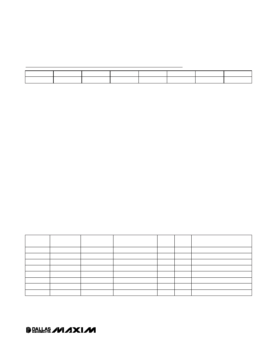
Table 3. CLK Input Frequency, Square-Wave Output Frequency
INTCN
CLKSEL1
CLKSEL0
INPUT FREQUENCY
RS2
RS1
SQUARE-WAVE OUTPUT
FREQUENCY
1
X
As selected
X
N/A (Interrupt)
0
32,768Hz
0
1Hz
0
32,768Hz
0
1
1.024kHz
0
32,768Hz
1
0
4.096kHz
0
32,768Hz
1
8.192kHz
0
1
8192Hz
X
1Hz
0
1
0
60Hz
X
1Hz
0
1
50Hz
X
1Hz
Bit 7
Bit 6
Bit 5
Bit 4
Bit 3
Bit 2
Bit 1
Bit 0
ECLK
CLKSEL1
CLKSEL0
RS2
RS1
INTCN
A2IE
A1IE
Control Register (0Eh)
相关PDF资料 |
PDF描述 |
|---|---|
| VI-J2Z-MZ | CONVERTER MOD DC/DC 2V 10W |
| ISL23418TFRUZ-T7A | IC DGTL POT 1CH 100K 10UTQFN |
| MS27473E24B35PB | CONN PLUG 128POS STRAIGHT W/PINS |
| VI-J2V-MZ | CONVERTER MOD DC/DC 5.8V 25W |
| VI-J2N-MZ | CONVERTER MOD DC/DC 18.5V 25W |
相关代理商/技术参数 |
参数描述 |
|---|---|
| DS1380N | 制造商:未知厂家 制造商全称:未知厂家 功能描述:NVRAM (Battery Based) |
| DS1380S | 制造商:未知厂家 制造商全称:未知厂家 功能描述:NVRAM (Battery Based) |
| DS1380SN | 制造商:未知厂家 制造商全称:未知厂家 功能描述:NVRAM (Battery Based) |
| DS1384 | 制造商:DALLAS 制造商全称:Dallas Semiconductor 功能描述:Watchdog Timekeeping Controller |
| DS1384FP | 制造商:MAXIM 制造商全称:Maxim Integrated Products 功能描述:Watchdog Timekeeping Controller |
发布紧急采购,3分钟左右您将得到回复。