- 您现在的位置:买卖IC网 > PDF目录9351 > DS17887-5IND+ (Maxim Integrated Products)IC RTC 5V 8K NV RAM 24-EDIP PDF资料下载
参数资料
| 型号: | DS17887-5IND+ |
| 厂商: | Maxim Integrated Products |
| 文件页数: | 18/31页 |
| 文件大小: | 0K |
| 描述: | IC RTC 5V 8K NV RAM 24-EDIP |
| 产品培训模块: | Lead (SnPb) Finish for COTS Obsolescence Mitigation Program |
| 标准包装: | 14 |
| 类型: | 时钟/日历 |
| 特点: | 警报器,夏令时,闰年,NVSRAM,方波输出 |
| 存储容量: | 8KB |
| 时间格式: | HH:MM:SS(12/24 小时) |
| 数据格式: | YY-MM-DD-dd |
| 接口: | 并联 |
| 电源电压: | 4.5 V ~ 5.5 V |
| 电压 - 电源,电池: | 2.5 V ~ 3.7 V |
| 工作温度: | -40°C ~ 85°C |
| 安装类型: | 通孔 |
| 封装/外壳: | 24-DIP 模块(0.600",15.24mm) |
| 供应商设备封装: | 24-EDIP |
| 包装: | 管件 |
第1页第2页第3页第4页第5页第6页第7页第8页第9页第10页第11页第12页第13页第14页第15页第16页第17页当前第18页第19页第20页第21页第22页第23页第24页第25页第26页第27页第28页第29页第30页第31页
Bit 7: Valid RAM and Time 2 (VRT2). This status bit
gives the condition of the auxiliary battery. It is set to
logic 1 condition when the external lithium battery is
connected to the VBAUX. If this bit is read as logic 0,
the external battery should be replaced.
Bit 6: Increment in Progress Status (INCR). This bit is
set to 1 when an increment to the time/date registers is
in progress and the alarm checks are being made.
INCR is set to 1 at 122s before the update cycle starts
and is cleared to 0 at the end of each update cycle.
Bit 5: Burst Mode Enable (BME). The burst mode
enable bit allows the extended user RAM address reg-
isters to automatically increment for consecutive reads
and writes. When BME is set to logic 1, the automatic
incrementing is enabled and when BME is set to a logic
0, the automatic incrementing is disabled.
Bit 3: Power Active-Bar Control (PAB). When this bit
is 0, the PWR pin is in the active low state. When this bit
is 1, the PWR pin is in the high-impedance state. The
user can write this bit to logic 1 or 0. If either WF and
WIE = 1 or KF and KSE = 1, the PAB bit is cleared to 0.
Bit 2: RAM Clear Flag (RF). This bit is set to logic 1
when a high-to-low transition occurs on the RCLR input
if RCE = 1. Writing this bit to logic 0 clears it. This bit
can also be written to logic 1 to force an interrupt con-
dition.
Bit 1: Wake-Up Alarm Flag (WF). This bit is set to 1
when a wake-up alarm condition occurs or when the
user writes it to 1. WF is cleared by writing it to 0.
Bit 0: Kickstart Flag (KF). This bit is set to 1 when a
kickstart condition occurs or when the user writes it to
1. This bit is cleared by writing it to logic 0.
Extended Control Registers
Two extended control registers are provided to supply
control and status information for the extended func-
tions offered by the DS17x85/DS17x87. These are des-
ignated as Extended Control Registers 4A and 4B, and
are located in register bank 1, locations 04AH and
04BH, respectively. The functions of the bits within
these registers are described as follows.
DS17285/DS17287/DS17485/DS17487/DS17885/DS17887
Real-Time Clocks
____________________________________________________________________
25
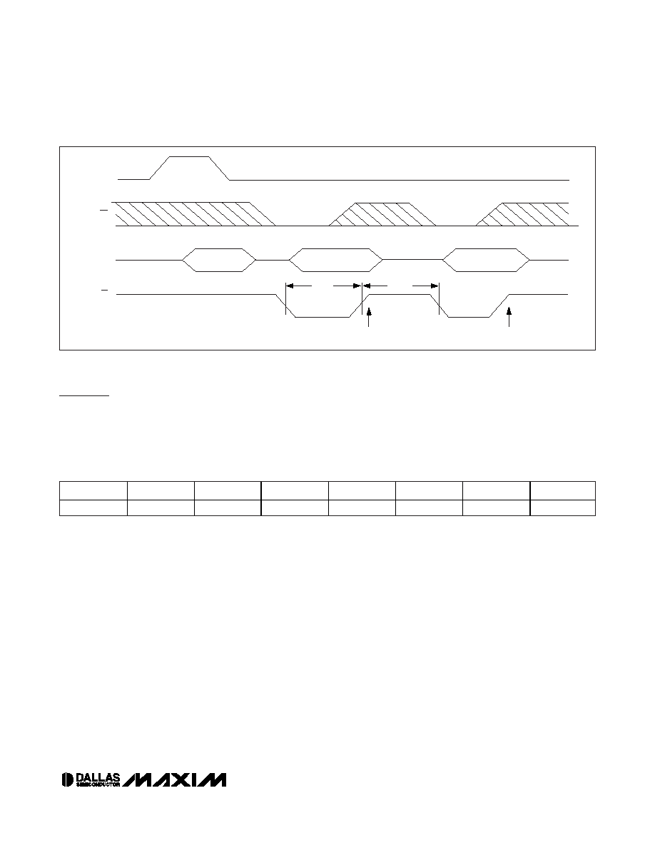
Figure 7. Burst Mode Timing Waveform
ADDRESS + 1
AS
53H
DATA
PWRWL
PWRWH
DATA
CS
AD0-7
DS OR R/W
ADDRESS + 2
*
Reserved bit. This bit is reserved for future use. It can be read and written, but has no effect on operation.
BIT 7
BIT 6
BIT 5
BIT 4
BIT 3
BIT 2
BIT 1
BIT 0
VRT2
INCR
BME
*
PAB
RF
WF
KF
Extended Control Register (4Ah)
MSB
LSB
相关PDF资料 |
PDF描述 |
|---|---|
| MCP4141-502E/SN | IC POT DGTL SNGL 5K SPI 8SOIC |
| DS1248WP-120IND+ | IC NVSRAM 1MBIT 120NS 34PCM |
| DS1248Y-70IND+ | IC NVSRAM 1MBIT 70NS 32DIP |
| DS1248W-120IND+ | IC NVSRAM 1MBIT 120NS 32DIP |
| DS1251W-120+ | IC NVSRAM 4MBIT 120NS 32DIP |
相关代理商/技术参数 |
参数描述 |
|---|---|
| DS17887-5IND+ | 功能描述:实时时钟 3V/5V RTC RoHS:否 制造商:Microchip Technology 功能:Clock, Calendar. Alarm RTC 总线接口:I2C 日期格式:DW:DM:M:Y 时间格式:HH:MM:SS RTC 存储容量:64 B 电源电压-最大:5.5 V 电源电压-最小:1.8 V 最大工作温度:+ 85 C 最小工作温度: 安装风格:Through Hole 封装 / 箱体:PDIP-8 封装:Tube |
| DS17H531D | 制造商:SANYO 制造商全称:Sanyo Semicon Device 功能描述:3-PHASE STEPPING SYSTEMS |
| DS17H531S | 制造商:SANYO 制造商全称:Sanyo Semicon Device 功能描述:3-PHASE STEPPING SYSTEMS |
| DS17H532D | 制造商:SANYO 制造商全称:Sanyo Semicon Device 功能描述:3-PHASE STEPPING SYSTEMS |
| DS17H532S | 制造商:SANYO 制造商全称:Sanyo Semicon Device 功能描述:3-PHASE STEPPING SYSTEMS |
发布紧急采购,3分钟左右您将得到回复。