- 您现在的位置:买卖IC网 > PDF目录1913 > DS1876T+T&R (Maxim Integrated Products)IC CTRLR SFP DUAL LDD 28TQFN PDF资料下载
参数资料
| 型号: | DS1876T+T&R |
| 厂商: | Maxim Integrated Products |
| 文件页数: | 10/69页 |
| 文件大小: | 0K |
| 描述: | IC CTRLR SFP DUAL LDD 28TQFN |
| 产品培训模块: | Lead (SnPb) Finish for COTS Obsolescence Mitigation Program |
| 标准包装: | 2,500 |
| 类型: | SFP 激光控制器 |
| 输入类型: | 逻辑 |
| 输出类型: | 逻辑 |
| 接口: | I²C |
| 电流 - 电源: | 10mA |
| 安装类型: | 表面贴装 |
| 封装/外壳: | 28-WFQFN 裸露焊盘 |
| 供应商设备封装: | 28-TQFN-EP(5x5) |
| 包装: | 带卷 (TR) |
第1页第2页第3页第4页第5页第6页第7页第8页第9页当前第10页第11页第12页第13页第14页第15页第16页第17页第18页第19页第20页第21页第22页第23页第24页第25页第26页第27页第28页第29页第30页第31页第32页第33页第34页第35页第36页第37页第38页第39页第40页第41页第42页第43页第44页第45页第46页第47页第48页第49页第50页第51页第52页第53页第54页第55页第56页第57页第58页第59页第60页第61页第62页第63页第64页第65页第66页第67页第68页第69页
18
Maxim Integrated
SFP Controller with Dual LDD Interface
DS1876
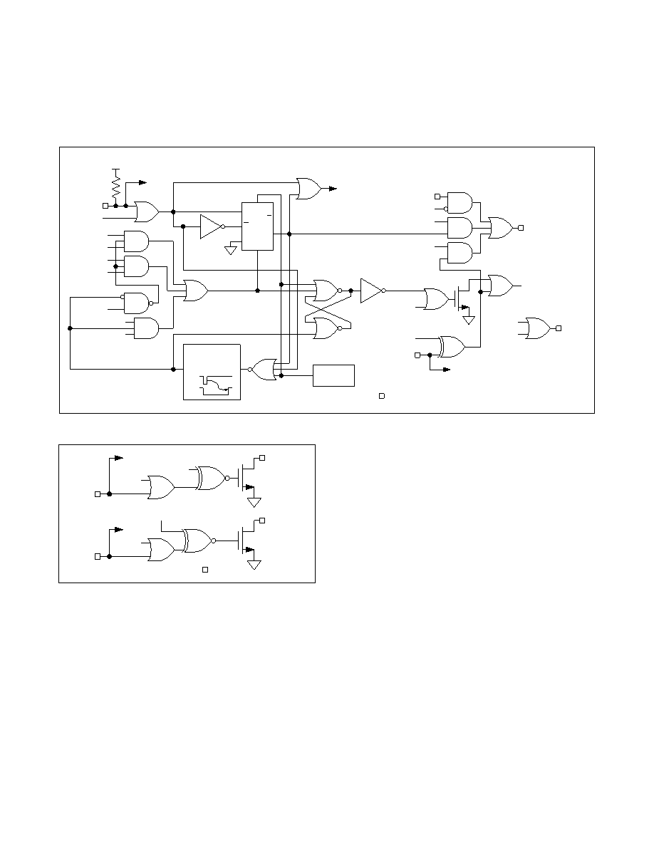
Digital I/O Pins
Six digital input pins and five digital output pins are pro-
vided for monitoring and control.
IN1, RSEL, OUT1, RSELOUT
Digital input pins IN1 and RSEL primarily serve to meet
the rate-select requirements of SFP and SFP+. They
can also serve as general-purpose inputs. OUT1 and
RSELOUT are driven by a combination of the IN1, RSEL,
and logic dictated by control registers in the EEPROM
(see Figure 10). The levels of IN1 and RSEL can be
read from the STATUS register (Lower Memory, Register
6Eh). The open-drain output OUT1 can be controlled
and/or inverted using the CNFGB register (Table 02h,
Register 89h). The open-drain RSELOUT output is
software controlled and/or inverted through the STATUS
register and CNFGA register (Table 02h, Register 88h).
External pullup resistors must be provided on OUT1 and
RSELOUT to realize high logic levels.
TXF1, TXF2, TXFOUT, TXD1, TXD2,
TXDOUT1, TXDOUT2
TXDOUT1 and TXDOUT2 are generated from a com-
bination of TXF1, TXF2, TXD1, TXD2, and the internal
signals FETG1 and FETG2 (Table 02h, Register 8Ah). A
software control identical to TXD1 and TXD2 is also avail-
able (TXDC1 and TXDC2, Lower Memory, Register 6Eh).
A TXD1 or TXD2 pulse is internally extended (TXDEXT)
by time tINITR1 to inhibit the latching of low alarms and
warnings related to the APC loop to allow for the loop to
stabilize. The nonlatching alarms and warnings are TXP
LO, BMON1 LO, BMON2 LO, PMON1 LO, and PMON2
LO. In addition, TXP LO is disabled from creating FETG.
See the Transmit Fault (TXFOUT) Output section for a
detailed explanation of TXFOUT. As shown in Figure 9,
the same signals and faults can also be used to gener-
ate the internal signal FETG. FETG is used to send a fast
“turn-off” command to the laser driver. The intended use
is a direct connection to the laser driver’s TXD1, TXD2
input if this is desired. When VCC < POA, TXDOUT1 and
TXDOUT2 are high impedance.
Figure 9. Logic Diagram 1
Figure 10. Logic Diagram 2
C
D
Q
S
R
OUT
IN
TXDS_
TXFS_
RPU
SET BIAS_ DAC AND
MOD_ DAC TO HIGH
IMPEDANCE
TXD_
TXFINT
INVTXF_
TXFOUTS1
TXFOUTS2
TXF_
TXP_ HI FLAG
TXP HI ENABLE
HBAL_ FLAG
HBAL ENABLE
QTHEXT_
TXP_ LO FLAG
TXP LO ENABLE
TXDEXT (tINITR1)
TXDC_
VCC
TXD_
TXDOUT_
TXFOUTS_
TXDIO_
TXDFG_
FETG_
TXDFLT_
FAULT RESET TIMER
(130ms)
IN
OUT
POWER-ON
RESET
TXFOUT
NOTE:
_ CAN BE EITHER 1 OR 2 CORRESPONDING TO TRANSMITTERS 1 OR 2.
REFERS TO A PIN.
INVOUT1
IN1C
IN1
IN1S
OUT1
INVRSOUT
RSELOUT
RSELC
RSEL
RSELS
= PINS
相关PDF资料 |
PDF描述 |
|---|---|
| DS1877T+T&R | IC CTLR/MON SFP 1-2CH 28TQFN |
| DS1878T+T&R | IC CTLR SFP W/DGTL LDD RX 28TQFN |
| DS1881Z-050+T&R | IC DGTL POT NV 2CH 45K 16-SOIC |
| DS1882Z-050+T&R | IC POT DIGIT DL LOG 50K 16SOIC |
| DS1884AT+T | IC SFP PON ONU CTRLR 24TQFN |
相关代理商/技术参数 |
参数描述 |
|---|---|
| DS1877 | 制造商:MAXIM 制造商全称:Maxim Integrated Products 功能描述:SFP Controller for Dual Rx Interface |
| DS1877T+ | 功能描述:ADC / DAC多通道 SFP+ Controller w/ Dual RX Interface RoHS:否 制造商:Texas Instruments 转换速率: 分辨率:8 bit 接口类型:SPI 电压参考: 电源电压-最大:3.6 V 电源电压-最小:2 V 最大工作温度:+ 85 C 安装风格:SMD/SMT 封装 / 箱体:VQFN-40 |
| DS1877T+T&R | 制造商:Maxim Integrated Products 功能描述:SFP CTRLR FOR DUAL RX INTERFACE TQF - Tape and Reel 制造商:Maxim Integrated Products 功能描述:IC CTLR/MON SFP 1-2CH 28TQFN |
| DS1877T+T&R | 功能描述:ADC / DAC多通道 SFP+ Controller w/ Dual RX Interface RoHS:否 制造商:Texas Instruments 转换速率: 分辨率:8 bit 接口类型:SPI 电压参考: 电源电压-最大:3.6 V 电源电压-最小:2 V 最大工作温度:+ 85 C 安装风格:SMD/SMT 封装 / 箱体:VQFN-40 |
| DS1877T+TR | 制造商:MAXIM 制造商全称:Maxim Integrated Products 功能描述:SFP Controller for Dual Rx Interface |
发布紧急采购,3分钟左右您将得到回复。