- 您现在的位置:买卖IC网 > PDF目录1914 > DS2143QN/T&R (Maxim Integrated Products)IC CONTROLLER E1 5V LP 44-PLCC PDF资料下载
参数资料
| 型号: | DS2143QN/T&R |
| 厂商: | Maxim Integrated Products |
| 文件页数: | 34/44页 |
| 文件大小: | 0K |
| 描述: | IC CONTROLLER E1 5V LP 44-PLCC |
| 产品培训模块: | Lead (SnPb) Finish for COTS Obsolescence Mitigation Program |
| 标准包装: | 500 |
| 控制器类型: | E1 控制器 |
| 接口: | 并行/串行 |
| 电源电压: | 4.5 V ~ 5.5 V |
| 电流 - 电源: | 10mA |
| 工作温度: | -40°C ~ 85°C |
| 安装类型: | 表面贴装 |
| 封装/外壳: | 44-LCC(J 形引线) |
| 供应商设备封装: | 44-PLCC(16.59x16.59) |
| 包装: | 带卷 (TR) |
第1页第2页第3页第4页第5页第6页第7页第8页第9页第10页第11页第12页第13页第14页第15页第16页第17页第18页第19页第20页第21页第22页第23页第24页第25页第26页第27页第28页第29页第30页第31页第32页第33页当前第34页第35页第36页第37页第38页第39页第40页第41页第42页第43页第44页
DS2143/DS2143Q
4 of 44
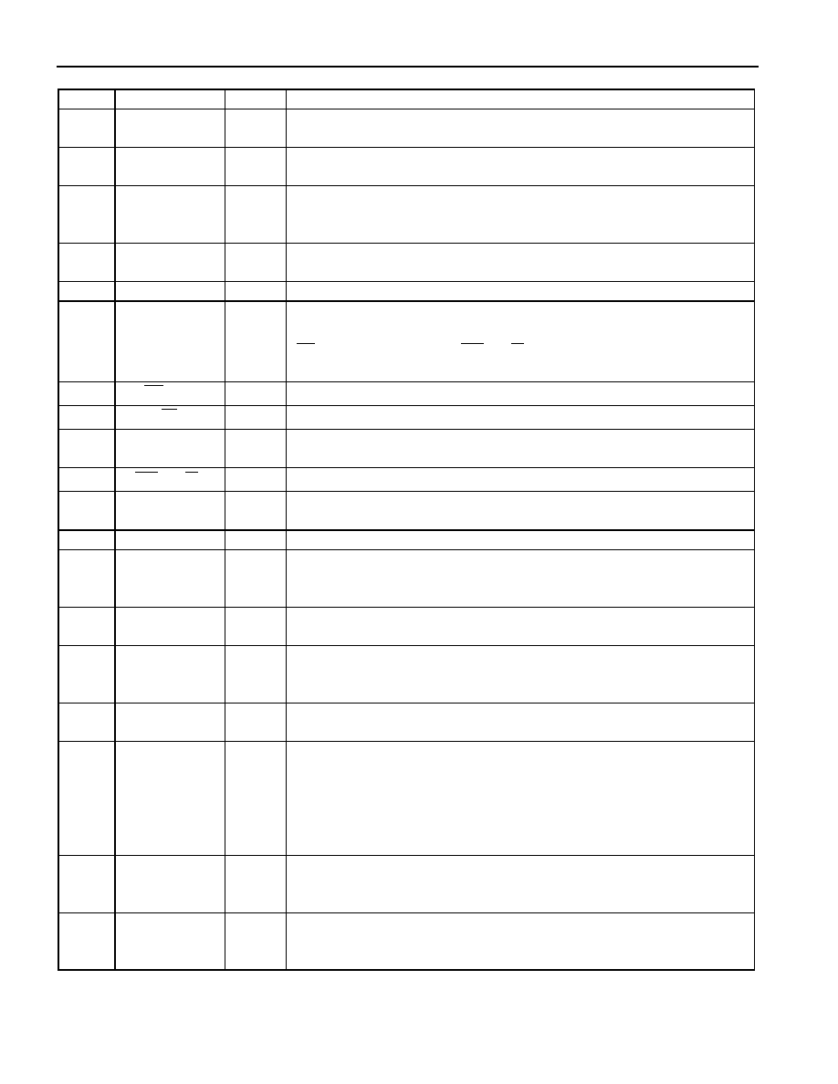
PIN DESCRIPTION Table 1
PIN
SYMBOL
TYPE
DESCRIPTION
1TCLK
I
Transmit Clock. 2.048 MHz primary clock. A clock must be
applied at the TCLK pin for the parallel port to operate properly.
2TSER
I
Transmit Serial Data. Transmit NRZ serial data, sampled on the
falling edge of TCLK.
3TCHCLK
O
Transmit Channel Clock. 256 kHz clock which pulses high during
the LSB of each channel. Useful for parallel-to-serial conversion of
channel data. See Section 13 for timing details.
4
5
TPOS
TNEG
O
Transmit Bipolar Data. Updated on rising edge of TCLK. For
optical links, can be programmed to output NRZ data.
6-13
AD0-AD7
I/O
Address/Data Bus. An 8-bit multiplexed address/data bus.
14
BTS
I
Bus Type Select. Strap high to select Motorola bus timing; strap
low to select Intel bus timing. This pin controls the function of
RD
(DS), ALE(AS), and WR (R/ W ) pins. If BTS=1, then these pins
assume the function listed in parentheses ().
15
RD
(DS)
I
Read Input (Data Strobe).
16
CS
I
Chip Select. Must be low to read or write the port.
17
ALE(AS)
I
Address Latch Enable (Address Strobe). A positive-going edge
serves to demultiplex the bus.
18
WR
(R/ W )
I
Write Input (Read/Write).
19
RLINK
O
Receive Link Data. Outputs Sa bits. See Section 13 for timing
details.
20
VSS
-
Signal Ground. 0.0 volts.
21
RLCLK
O
Receive Link Clock. 4 kHz to 20 kHz demand clock for the
RLINK output. Controlled by RCR2. See Section 13 for timing
details.
22
RCLK
I
Receive Clock. 2.048 MHz primary clock. A clock must be applied
at the RCLK pin for the parallel port to operate properly.
23
RCHCLK
O
Receive Channel Clock. 256 kHz clock which pulses high during
the LSB of each channel. Useful for serial to parallel conversion of
channel data. See Section 13 for timing details.
24
RSER
O
Receive Serial Data. Received NRZ serial data, updated on rising
edges of RCLK.
25
RSYNC
I/O
Receive Sync. An extracted pulse, one RCLK wide, is output at this
pin which identifies either frame (RCR1.6=0) or multiframe
boundaries (RCR1.6=1). If the elastic store is enabled via the
RCR2.1, then this pin can be enabled to be an input via RCR1.5 at
which a frame boundary pulse is applied. See Section 13 for timing
details.
26
27
RPOS
RNEG
I
Receive Bipolar Data Inputs. Sampled on falling edge of RCLK.
Tie together to receive NRZ data and disable BPV monitoring
circuitry.
28
SYSCLK
I
System Clock. 1.544 MHz or 2.048 MHz clock. Only used when
the elastic store function is enabled via the RCR2.1. Should be tied
low in applications that do not use the elastic store.
相关PDF资料 |
PDF描述 |
|---|---|
| DS21448L | IC LIU QUAD E1/T1/J1 128-LQFP |
| DS21455N+ | IC LIU QUAD T1/E1/J1 256-BGA |
| DS2148GN+ | IC LIU E1/T1/J1 3.3V/5V 49-BGA |
| DS2148T | IC LIU E1/T1/J1 5V 44-TQFP |
| DS2149Q+ | IC LIU T1/J1 5V 28-PLCC |
相关代理商/技术参数 |
参数描述 |
|---|---|
| DS21448 | 功能描述:网络控制器与处理器 IC 3.3V E1/T1/J1 Quad Interface RoHS:否 制造商:Micrel 产品:Controller Area Network (CAN) 收发器数量: 数据速率: 电源电流(最大值):595 mA 最大工作温度:+ 85 C 安装风格:SMD/SMT 封装 / 箱体:PBGA-400 封装:Tray |
| DS21448A1 | 功能描述:网络控制器与处理器 IC 3.3V E1/T1/J1 Quad Interface RoHS:否 制造商:Micrel 产品:Controller Area Network (CAN) 收发器数量: 数据速率: 电源电流(最大值):595 mA 最大工作温度:+ 85 C 安装风格:SMD/SMT 封装 / 箱体:PBGA-400 封装:Tray |
| DS21448DK | 功能描述:网络开发工具 DS21448 Dev Kit RoHS:否 制造商:Rabbit Semiconductor 产品:Development Kits 类型:Ethernet to Wi-Fi Bridges 工具用于评估:RCM6600W 数据速率:20 Mbps, 40 Mbps 接口类型:802.11 b/g, Ethernet 工作电源电压:3.3 V |
| DS21448G+ | 功能描述:网络控制器与处理器 IC 3.3V E1/T1/J1 Quad Interface RoHS:否 制造商:Micrel 产品:Controller Area Network (CAN) 收发器数量: 数据速率: 电源电流(最大值):595 mA 最大工作温度:+ 85 C 安装风格:SMD/SMT 封装 / 箱体:PBGA-400 封装:Tray |
| DS21448GN+ | 功能描述:网络控制器与处理器 IC 3.3V E1/T1/J1 Quad Interface RoHS:否 制造商:Micrel 产品:Controller Area Network (CAN) 收发器数量: 数据速率: 电源电流(最大值):595 mA 最大工作温度:+ 85 C 安装风格:SMD/SMT 封装 / 箱体:PBGA-400 封装:Tray |
发布紧急采购,3分钟左右您将得到回复。