- 您现在的位置:买卖IC网 > PDF目录1914 > DS21448L (Maxim Integrated Products)IC LIU QUAD E1/T1/J1 128-LQFP PDF资料下载
参数资料
| 型号: | DS21448L |
| 厂商: | Maxim Integrated Products |
| 文件页数: | 2/60页 |
| 文件大小: | 0K |
| 描述: | IC LIU QUAD E1/T1/J1 128-LQFP |
| 产品培训模块: | Lead (SnPb) Finish for COTS |
| 产品变化通告: | Product Discontinuation 20/Feb/2012 |
| 标准包装: | 72 |
| 类型: | 线路接口装置(LIU) |
| 驱动器/接收器数: | 4/4 |
| 规程: | T1/E1/J1 |
| 电源电压: | 3.135 V ~ 3.465 V |
| 安装类型: | 表面贴装 |
| 封装/外壳: | 128-LQFP |
| 供应商设备封装: | 128-LQFP(14x20) |
| 包装: | 管件 |
第1页当前第2页第3页第4页第5页第6页第7页第8页第9页第10页第11页第12页第13页第14页第15页第16页第17页第18页第19页第20页第21页第22页第23页第24页第25页第26页第27页第28页第29页第30页第31页第32页第33页第34页第35页第36页第37页第38页第39页第40页第41页第42页第43页第44页第45页第46页第47页第48页第49页第50页第51页第52页第53页第54页第55页第56页第57页第58页第59页第60页
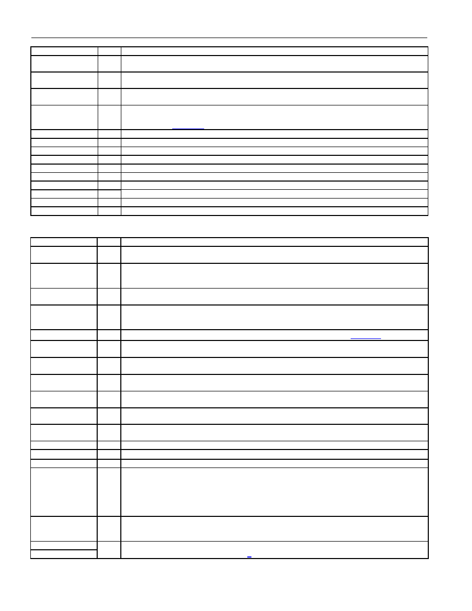
DS21448 3.3V T1/E1/J1 Quad Line Interface
10 of 60
PIN
I/O
FUNCTION
RCLK1–RCLK4
O
Receive Clock. Buffered recovered clock from the line. Synchronous to MCLK in absence of
signal at RTIP and RRING.
TPOS1–TPOS4
I
Transmit Positive Data. Sampled on the falling edge (CCR2.1 = 0) or the rising edge
(CCR2.1 = 1) of TCLK for data to be transmitted out onto the line.
TNEG1–TNEG4
I
Transmit Negative Data. Sampled on the falling edge (CCR2.1 = 0) or the rising edge
(CCR2.1 = 1) of TCLK for data to be transmitted out onto the line.
TCLK1–TCLK4
I
Transmit Clock. A 2.048MHz or 1.544MHz primary clock. It is used to clock data through the
transmit-side formatter. It can be sourced internally by MCLK or RCLK. See Common Control
Register 1 and Figure 1-3.
JTRST
I
JTAG Reset
JTMS
I
JTAG Mode Select
JTCLK
I
JTAG Clock
JTDI
I
JTAG Data In
JTDO
O
JTAG Data Out
VSM
I
Voltage Supply Mode (LQFP only). Should be wired low for correct operation.
TVDD1–TVDD4
—
3.3V, ±5% Transmitter Positive Supply
VDD1–VDD4
—
3.3V, ±5% Positive Supply
TVSS1–TVSS4
—
Transmitter Signal Ground
VSS1–VSS4
—
Signal Ground
Table 2-D. Serial Interface Mode Pin Description
PIN
I/O
FUNCTION
INT
I/O
Interrupt (
INT). Flags host controller during conditions and change of conditions defined in the
status register. Active-low, open-drain output.
TXDIS/TEST
I
Tri-State Control, Multifunctional. Set this pin high with all
CS1–CS4 inputs inactive to tri-state
TTIP1–TTIP4 and TRING1–TRING4. Set this pin high with any of the
CS1–CS4 inputs active to
tri-state all outputs and I/O pins (including the parallel control port). Set low for normal operation.
HRST
I
Hardware Reset. Bringing
HRST low resets the DS21448, setting all control bits to the all-zeros
default state.
MCLK
I
Master Clock. A 2.048MHz (±50ppm) clock source with TTL levels is applied at this pin. This
clock is used internally for both clock/data recovery and for jitter attenuation. A T1 1.544MHz
clock source is optional (Note 1).
BIS0/BIS1
I
Bus Interface Select Bit 0 and 1. Used to select bus interface option. See Table 2-A for details.
CS1
I
Chip Select 1. Must be low to read or write to channel 1 of the device.
CS1 is an active-low
signal.
CS2
I
Chip Select 2. Must be low to read or write to channel 2 of the device.
CS2 is an active-low
signal.
CS3
I
Chip Select 3. Must be low to read or write to channel 3 of the device.
CS3 is an active-low
signal.
CS4
I
Chip Select 4. Must be low to read or write to channel 4 of the device.
CS4 is an active-low
signal.
ICES
I
Input Clock-Edge Select. Selects whether the serial interface data input (SDI) is sampled on the
rising (ICES = 0) or falling edge (ICES = 1) of SCLK.
OCES
I
Output Clock-Edge Select. Selects whether the serial interface data output (SDO) changes on
the rising (OCES = 1) or falling edge (OCES = 0) of SCLK.
SCLK
I
Serial Clock. Serial interface clock.
SDI
I
Serial Data Input. Serial interface data input.
SDO
O
Serial Data Output. Serial interface data output.
PBEO1–PBEO4
O
PRBS Bit-Error Output. The receiver constantly searches for a 2
15 - 1 (E1) or a QRSS (T1)
PRBS, depending on the ETS bit setting (CCR1.7). It remains high if it is out of synchronization
with the PRBS pattern. It goes low when synchronized to the PRBS pattern. Any errors in the
received pattern after synchronization cause a positive-going pulse (with same period as E1 or
T1 clock) synchronous with RCLK. PRBS bit errors can also be reported to the ECR1 and ECR2
registers by setting CCR6.2 to logic 1.
RCL1/LOTC1–
RCL4/LOTC4
O
Receive Carrier Loss/Loss-of-Transmit Clock. An output that toggles high during a receive carrier
loss (CCR2.7 = 0) or toggles high if the TCLK pin has not been toggled for 5
s ± 2s
(CCR2.7 = 1). CCR2.7 defaults to logic 0 when in hardware mode.
RTIP1–RTIP4
RRING1–RRING4
I
Receive Tip and Ring. Analog inputs for clock recovery circuitry. These pins connect through a
1:1 transformer to the line. See Section 7 for details.
相关PDF资料 |
PDF描述 |
|---|---|
| DS21455N+ | IC LIU QUAD T1/E1/J1 256-BGA |
| DS2148GN+ | IC LIU E1/T1/J1 3.3V/5V 49-BGA |
| DS2148T | IC LIU E1/T1/J1 5V 44-TQFP |
| DS2149Q+ | IC LIU T1/J1 5V 28-PLCC |
| DS2151QN | IC TXRX T1 1-CH 5V LP IND 44PLCC |
相关代理商/技术参数 |
参数描述 |
|---|---|
| DS21448L+ | 功能描述:网络控制器与处理器 IC 3.3V E1/T1/J1 Quad Interface RoHS:否 制造商:Micrel 产品:Controller Area Network (CAN) 收发器数量: 数据速率: 电源电流(最大值):595 mA 最大工作温度:+ 85 C 安装风格:SMD/SMT 封装 / 箱体:PBGA-400 封装:Tray |
| DS21448L+W | 功能描述:网络控制器与处理器 IC 3.3V E1/T1/J1 Quad Interface RoHS:否 制造商:Micrel 产品:Controller Area Network (CAN) 收发器数量: 数据速率: 电源电流(最大值):595 mA 最大工作温度:+ 85 C 安装风格:SMD/SMT 封装 / 箱体:PBGA-400 封装:Tray |
| DS21448LDK | 功能描述:KIT DESIGN LIU DS21448L T1/J1/E1 RoHS:否 类别:编程器,开发系统 >> 过时/停产零件编号 系列:- 标准包装:1 系列:- 传感器类型:CMOS 成像,彩色(RGB) 传感范围:WVGA 接口:I²C 灵敏度:60 fps 电源电压:5.7 V ~ 6.3 V 嵌入式:否 已供物品:成像器板 已用 IC / 零件:KAC-00401 相关产品:4H2099-ND - SENSOR IMAGE WVGA COLOR 48-PQFP4H2094-ND - SENSOR IMAGE WVGA MONO 48-PQFP |
| DS21448LN | 功能描述:网络控制器与处理器 IC 3.3V E1/T1/J1 Quad Interface RoHS:否 制造商:Micrel 产品:Controller Area Network (CAN) 收发器数量: 数据速率: 电源电流(最大值):595 mA 最大工作温度:+ 85 C 安装风格:SMD/SMT 封装 / 箱体:PBGA-400 封装:Tray |
| DS21448LN+ | 功能描述:网络控制器与处理器 IC 3.3V E1/T1/J1 Quad Interface RoHS:否 制造商:Micrel 产品:Controller Area Network (CAN) 收发器数量: 数据速率: 电源电流(最大值):595 mA 最大工作温度:+ 85 C 安装风格:SMD/SMT 封装 / 箱体:PBGA-400 封装:Tray |
发布紧急采购,3分钟左右您将得到回复。